
Professional PCB manufacturing and assembly
Building 6, Zone 3, Yuekang Road,Bao'an District, Shenzhen, China
+86-13410863085Mon.-Sat.08:00-20:00

1. Pcb design should not stop at the input of basic schematic diagram
Schematic diagram input is very important for generating the logical connection of pcb design. it must be accurate, simple and easy to use and integrated with planning to ensure the success of design.
Simply entering a schematic and transferring it to the plan is not enough. In order to create a high-quality design that meets the expectations, it is necessary to ensure that the best components are used and that simulation analysis can be performed, so as to ensure that the pcb design will not have problems when entrusted to manufacturing.
2. Pcb design should not ignore the library management library
Management is an important part of the design process. In order to quickly select the best PCB components and place them in the pcb design, the simple creation and easy management of components become very necessary.
PADS allows you to maintain all design tasks in a library and update the library in real time to facilitate application and ensure the accuracy of design and development. You can access all information through a single table without worrying about data redundancy, multiple libraries, or time-consuming tool spending.
3. Effectively manage pcb design constraint rules
Today's key high-speed design is extremely complex. If there is no effective means to manage constraint rules, the design, constraint and management of routing, topology and signal delay will become extremely difficult. In order to build a successful product in the first iteration, constraint rules must be set early in the design process so that the design can reach the purpose of the request. Good constraint rule management can prevent you from using expensive or unavailable components, and ultimately ensure that the circuit board meets the performance and manufacturing requirements.
4. Ensure that you have the required pcb design planning talents
In recent years, the complexity of pcb planning and design is significantly higher than before. In order to make pcb smaller and more portable electronic installation, the density of PCB design has to be improved. In addition, the working frequency has also been improved, which requires designers to evaluate features that may have been overlooked before to ensure that the design is available. In order to keep up with the increasing complexity, pcb designers must have a more general ability to define high-level rule sets, create common rf profiles and implement correction structures to improve the overall performance of the design.
In the planning process, pcb design intelligent planning tools help to create efficient layout and routing strategies. Fine layout can reduce the violations in the later stage of design, so that you can complete the project more quickly with fewer mistakes.
Although manual routing is commonly used to achieve the real pcb design intent, the effective combination of interactive routing and automatic routing can help meet the market time limit requirements and improve the design quality. Automatic routing can also help deal with difficult tasks, such as differential pair routing, network adjustment, manufacturing optimization, micro via and layer adding technology. If the cabling strategy is planned in advance, the efficiency of using automatic cabling will be greatly improved.
Another challenge is that modern pcb design needs to maintain thousands of networks, which may bring difficulties to the routing of key areas in the design. The best way to prevent this problem is to divide the network cable into dividend groups in order to create an effective cabling strategy. After the planning group is created, the network group can be marked and filtered to highlight the key networks requiring PCB wiring.
A series of problems to be checked in pcb design
Nov 19,2022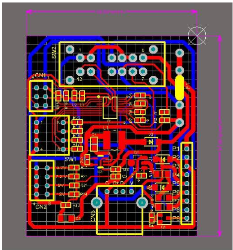


Just upload Gerber files, BOM files and design files, and the KINGFORD team will provide a complete quotation within 24h.