
Professional PCB manufacturing and assembly
Building 6, Zone 3, Yuekang Road,Bao'an District, Shenzhen, China
+86-13410863085Mon.-Sat.08:00-20:00


Components and solder joints related to PCB chip soldering
PCB welding is an important process in electronic product assembly Welding quality directly affects the efficiency of electronic circuits and electronic devices
Excellent welding quality can provide good stability and reliability for the circuit. Poor welding methods will lead to component damage, bring great difficulties to testing, and sometimes leave hidden dangers that affect the reliability of electronic equipment.
1. Classification and characteristics of PCB chip welding
Welding is generally divided into three categories: fusion welding, contact welding and welding.
Fusion welding: refers to the method of heating the weldment joint to the molten state during welding and completing welding without applying pressure. Such as electric arc welding, gas welding, etc.
Contact welding: During welding, pressure must be applied to the weldment (heated or unheated) to complete the welding. Such as ultrasonic welding, pulse welding, friction welding, etc.
Soldering: The so-called "soldering" during the installation of electronic products is a kind of soft soldering, which mainly uses low melting point alloy materials such as tin and lead as solder, so it is commonly known as "soldering".
Second, principle PCB chip welding
Welding of electronic circuits seems simple. It seems that it is just a process of combining the molten solder with the metal (base metal) to be welded, but its micro mechanism is very complex, involving physics, chemistry, material science, electricity and other knowledge. Familiar with the basic theory of welding, you can understand various problems in welding and freely deal with them, so as to improve the welding quality of welding joints.
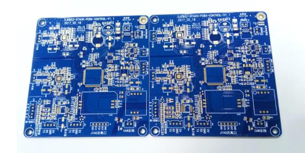
Circuit board

Welding is the process of heating the solder and the metal to be welded to the optimal temperature at the same time, melting the solder to fill the gap between the metals and form a metal alloy combination with them. From the microscopic point of view, welding includes two processes: one is the wetting process, and the other is the diffusion process.
1. Wetting (lateral flow)
Also called wetting, it means that the molten solder forms a uniform, smooth, continuous and firmly adhered solder layer on the metal surface.
The wettability is mainly determined by the cleanliness of the weldment surface and the surface tension of the solder.
The metal surface looks relatively smooth, but under the microscope, there are countless inhomogeneities, grain boundaries and scars. Solder is wetted and diffused along the bumps and scars on these surfaces by capillary action. This welding should make the solder flow.
The flow process is usually that rosin removes the oxide film in front of it, and the solder follows it. The wetting is basically that the molten solder flows laterally along the object surface.
2. Diffusion (vertical flow)
As the molten solder diffuses on the surface to be welded, the solder diffuses into the solid metal. For example, when tin lead solder is used to weld copper parts, there are surface diffusion, grain boundary diffusion and intra particle diffusion in the welding process. Lead in tin lead solders only participates in surface diffusion, while tin and mace atoms diffuse each other, which is a selective diffusion determined by the properties of different metals. It is precisely because of this diffusion that a new alloy is formed on the interface between the two, so that the solder and the weldment can be firmly combined.
3. Metallurgical combination
Due to diffusion, an alloy layer is formed at the joint of tin atom and copper metal to be welded, thus forming a firm solder joint. Take tin lead solder soldering copper parts as an example. At low temperature (250 300 ℃), Cu3Sn and Cu6Sn5 will be formed at the interface between copper and solder. If the temperature exceeds 300 ℃, in addition to these alloys, intermetallic compounds such as Cu31Sn8 will also be formed. The thickness of solder joint interface varies with temperature and welding time, generally between 3~10um.
Elements of PCB patch welding
1. Weldability of welding base metal
Solderability means that the liquid solder and the base metal should be able to dissolve each other, that is, there must be a good affinity between the two atoms. The degree of mutual melting of two different metals depends on the atomic radius, their position in the periodic table and the type of crystal. Tin lead solders are mostly miscible with other metal materials, except that metal materials containing a large amount of chromium and aluminum alloys are not easy to dissolve each other. In order to improve solderability, measures such as surface tin plating and silver plating are usually adopted.
2. Cleanliness of weldments
The surface of solder and base metal must be "clean", where "clean" means there is no oxide layer between solder and base metal, let alone pollution. When there is oxide or dirt between the solder and the metal to be welded, it will hinder the free diffusion of the molten metal atoms and will not produce the wetting effect. Oxidation of component pins or PCB pads is one of the main reasons for "virtual soldering".
3. Flux
Flux can destroy the oxide film, purify the welding surface, and make the solder joints smooth and bright. The flux used in electronic assembly is usually rosin.
4. Welding temperature and time
The optimum welding temperature is 250 ± 5oC, and the minimum welding temperature is 240oC. The temperature is too low to form cold solder joints. When the temperature is higher than 260 ℃, the quality of solder joints will deteriorate.
Welding time: two processes of wetting and diffusion are completed in 2~3s, and only 35% of the two processes are completed in 1s. Generally, the welding time of integrated circuit and triode is less than 3s, and that of other components is 4-5s.
5. Welding method
Welding methods and procedures are critical.
Quality standard of PCB chip solder joint
1. Good power efficiency
High quality solder joints shall form a solid alloy layer on the surface of solder and metal workpiece to ensure good conductivity. During welding, it is prohibited to simply stack the solder on the surface of the metal workpiece to form a virtual weld.
2. Have certain mechanical strength
Electronic equipment sometimes needs to work in a vibration environment. In order to prevent the weldment from loosening or falling off, the welding point must have a certain mechanical strength. The strength of tin and lead in tin lead solder is relatively low. In order to increase the strength, additional welding surfaces can be added as required. Or, before welding, mesh, twist and hook the component lead and wire.
The amount of solder on the solder joint shall be appropriate
Too little solder on the solder joint will not only reduce the mechanical strength, but also lead to early failure of the solder joint; Too much solder on the solder joint will increase costs, easily lead to solder joint bridging (short circuit), and will also hide welding defects. In this case, the amount of solder on the solder joint shall be appropriate. When soldering a printed circuit board, it is most appropriate when the solder fills the pad and unfolds in a skirt shape.
4. The surface of welding spot shall be bright and uniform
The surface of good solder joints shall be bright and uniform in color. This is mainly because the film formed by the resin component that is not completely volatilized in the flux covers the solder joint surface, which can prevent the solder joint surface from oxidation.
5. The welding point shall be free of burrs and cavities
There are burrs and gaps on the surface of the solder joint, which is not only ugly, but also harmful to electronic products. Especially in the high-voltage circuit, it will cause severe discharge and damage electronic equipment.
6. PCB solder joint surface must be clean
If the dirt on the surface of the solder joint is not removed in time, acidic substances will corrode component wires, contacts and PCB, and moisture absorption will cause leakage or even short circuit combustion, causing serious hidden dangers
The above is the explanation given by the editor of pcb circuit board company.
If you want to know more about PCBA, you can go to our company's home page to learn about it.
In addition, our company also sells various circuit boards,
High frequency circuit board and SMT chip are waiting for your presence again.


Just upload Gerber files, BOM files and design files, and the KINGFORD team will provide a complete quotation within 24h.