
Professional PCB manufacturing and assembly
Building 6, Zone 3, Yuekang Road,Bao'an District, Shenzhen, China
+86-13410863085Mon.-Sat.08:00-20:00


Understand LCD controller
With the continuous development of display technology, true color LCD has gradually occupied an important position in PCB embedded display system with its advantages of high resolution, high contrast and high definition At present, the design and development of LCD controller based on PCB embedded platform mainly have two implementation channels: ARM embedded LCD controller and independent control device However, both implementations have shortcomings The use of embedded controller may add PCB processor and limit the display screen playback rate External PCB control equipment is not only expensive, but also very specific, which is difficult Adapt to different types of LCD screens
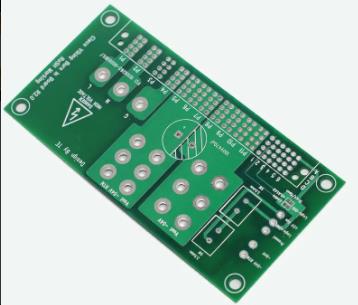
Circuit board

To solve this problem, this paper proposes a design scheme of LCD controller based on ARM and FPGA. On the one hand, this design scheme can improve the write rate of video memory and reduce the burden of processor by operating the frame buffer device under LINUX operating system. On the one hand, FPGA is used to realize the design of LCD controller, with short development cycle, low power consumption and strong portability, which can be applied to different small and medium-sized LCD screens.
The system is mainly composed of microcontroller, FPGA (LCD controller), memory unit and peripheral interface. The system block diagram is shown in Figure 1.
Working process of the system: Under the action of the timing control signal generated by the timing generation circuit inside the FPGA, the LCD controller reads the data required for display from the microcontroller through the frame buffer interface and stores it in the display buffer SRAM. At the same time, the LCD reads the display data from the display memory SRAM, and directly displays the data information in real time through the data format conversion circuit.
LCD controller is implemented based on FPGA. This program uses Altera's Cvclone (hurricane) series EPlC6Q240. FPGA has a high-speed data transmission I/O interface, which can achieve high-speed display memory read rate and greatly improve the LCD display screen playback rate. At the same time, FPGA is a programmable logic device, which can realize complex logic operations and provide complex control timing. LQ035Q3DG01 TFT-LCD LCD is adopted, with a resolution of 320 times; 240, the image signal is in RGB format.
Because SRAM has a higher read and write speed, this display buffer PCB design uses an IS61LV51216AL SRAM with a capacity of 512 KB, and the read and write speed is about 10ns And the size of displaying a frame of image is 125 KB (320x240x2/l024). The read/write speed of FPGA to display memory is about 200 nanoseconds, which meets the system requirements
The main control unit designed and developed by the controller uses AT9lRM9200 (9200 for short) of ATMEL Company as the microcontroller. The PCB processor is based on the ARM920T core, and the operating frequency is 180 MHz. The performance can reach 200mi/s, and the system adopts the open-source LINUX operating system. However, as the control terminal of the system, ARM9 needs to complete multiple tasks such as information collection, processing and external communication. If the LCD controller also reads data from memory for display, this will increase the burden on the processor and reduce the display cache. The rate of reading data will affect the real-time display of LCD. This paper proposes an application method based on the frame buffer interface under the LINUX operating system, which greatly improves the rate of reading data from the display memory, thus improving the real-time performance of the entire display system. Figure 3 shows the circuit connection of AT91RM9200 interface.
The software design of the system is mainly divided into two parts: LCD controller design based on FPGA and frame buffer driver design under LINUX operating system.
The LCD controller in this design is mainly composed of cache read/write, MCU interface and LCD timing control modules.
According to TFT-LCD display principle, the main control signals required for display include count clock signal, line/field synchronization PCB signal and enable signal. The resolution of the LCD screen in this scheme is 320x240. The refresh rate of the LCD screen needs to be designed as 60 Hz, that is, the VSYNC signal is 60 Hz. It is composed of line synchronization signal, the period of line synchronization signal is 1/(60x240) s, and then the line synchronization signal (HSYNC) is 15 kHz. Similarly, the point clock signal (CK) is 5MHz.
The FPGA contains a phase-locked loop IP module (PLL) to use the FPGA 50 MHz clock signal F_ CLK is divided by 10 to get 5 MHz point clock signal. The state machine method is used to design the timing control module with Verilog hardware description language, and PCB control signals VSYNC, HSYNC and ENAB that meet the timing requirements of LCD are provided. After the PCB design is completed, the timing simulation is completed in the QuatuslI environment, and the simulation results meet the timing requirements.
SRAM is a video storage module It can be seen that the transmission between the PCB data LCD controller and the microcontroller is read under the control of the ARM clock. When the LCD screen reads data from the SRAM under the control of the count clock signal CK, the following problems are addressed: the transmission between clock domains when PCB data are different, this scheme uses FPGA design to achieve asynchronous FIFO to complete


Just upload Gerber files, BOM files and design files, and the KINGFORD team will provide a complete quotation within 24h.