
Professional PCB manufacturing and assembly
Building 6, Zone 3, Yuekang Road,Bao'an District, Shenzhen, China
+86-13410863085Mon.-Sat.08:00-20:00


High frequency circuit board and PCB manufacturing and packaging
High frequency circuit board wiring
The shorter the lead between pins 1, the better the high-frequency circuit board device
The radiation intensity of the signal is proportional to the track length of the signal line. The longer the high-frequency signal wire is, the easier it is to couple with the components close to it. This requires that signals such as clock, crystal oscillator, DDR data, LVDS cable, USB cable, HDMI cable and other high-frequency signal cables be as short as possible.
2. The less lead layer alternation between pins of high-frequency circuit components, the better
The so-called "less interlaminar alternating of the leads, the better" means that the fewer vias used in the component connection process, the better. From the side, a through-hole can generate 0.5pF distributed capacitance. Reducing the number of through-holes can significantly improve the speed and reduce the possibility of data errors.
3. Pay attention to the "crosstalk" introduced by close parallel signal lines
High frequency circuit wiring shall pay attention to the "crosstalk" caused by close parallel wiring of signal lines. Crosstalk refers to the coupling between signal lines that are not directly connected. Since the high-frequency signal is transmitted along the transmission line in the form of electromagnetic wave, this signal line will act as an antenna, and the energy of electromagnetic field will be transmitted around the transmission line. Due to the mutual coupling of electromagnetic fields between signals, unwanted noise signals will be generated. It is called crosstalk. The parameters of PCB layer, the spacing of signal lines, the power characteristics of driver and receiver, and the termination method of signal lines all have certain effects on crosstalk. In order to reduce the crosstalk of high-frequency signals, the following points should be done as far as possible during wiring:
If the wiring space allows, inserting a ground wire or ground plane between two conductors with more serious crosstalk can isolate and reduce crosstalk.
When there is time-varying electromagnetic field in the space around the signal line, if parallel distribution cannot be avoided, a large area of "ground" can be arranged on the other side of the parallel signal line to greatly reduce interference.
If the wiring space allows, increase the spacing between adjacent signal lines, reduce the parallel length of signal lines, and try to make the clock lines perpendicular to the key signal lines instead of parallel.
If it is almost impossible to avoid parallel routing in the same layer, the routing directions in two adjacent layers must be perpendicular to each other.
In digital circuits, the usual clock signal is a signal with fast edge change and high external crosstalk. This, in the design, the clock wire should be surrounded by the ground wire, and more ground wire holes should be punched out to reduce the distributed capacitance, thus reducing crosstalk.
For high-frequency signal clock, try to use low-voltage differential clock signal and package grounding mode, and pay attention to the integrity of package grounding hole.
Unused input terminals should not be suspended in the air, but should be grounded or connected to the power supply (the power supply is also grounded in the high-frequency signal loop), because the suspended wire may be equivalent to the transmission antenna, and grounding can inhibit transmission. Practice has proved that using this method to eliminate crosstalk can sometimes produce immediate results.
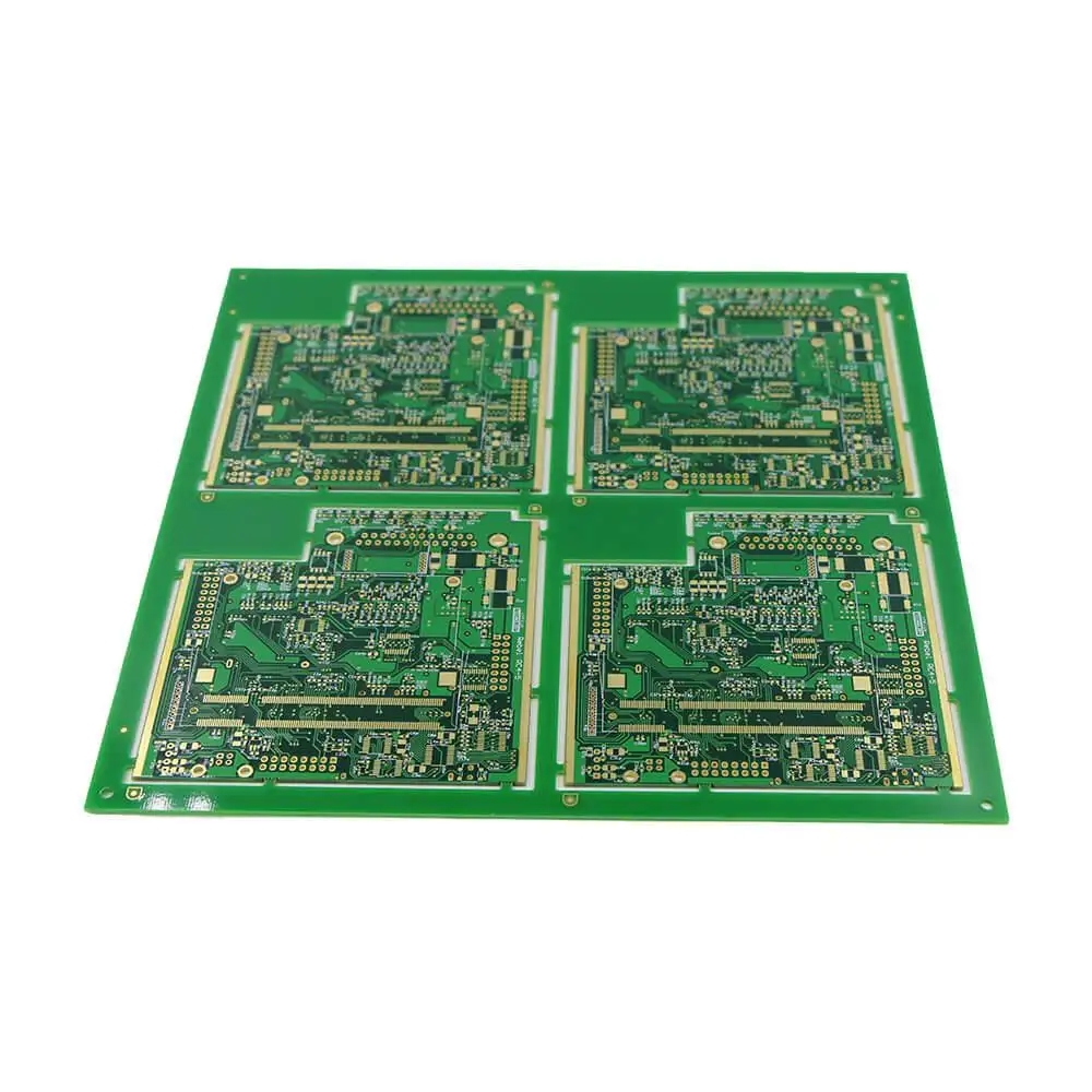
Circuit board

4. Add a high-frequency decoupling capacitor to the power supply pin of the integrated circuit block
A high-frequency decoupling capacitor is added to the power supply pin of each integrated circuit block nearby. The newly added high-frequency decoupling capacitor of the power supply pin can effectively suppress the interference of high-frequency harmonics on the power supply pin.
PCB design and manufacturing package
1. Accelerate and improve PCB wiring
Traditional PCB routing is limited by fixed wire coordinates and the lack of any angle wire. Eliminating these limitations can significantly improve wiring quality. This paper will introduce the advantages of arbitrary angle routing, flexible routing and a new algorithm for constructing Steiner tree through examples.
2. What problems should be paid attention to when drawing PCB from the perspective of welding?
Although there are more complex placement machines that can replace manual welding, there are too many factors that affect the welding quality. This paper introduces several problems that should be paid attention to when designing PCB from the point of view of SMT welding. According to experience, if these requirements are not followed, it is likely to lead to poor welding quality, faulty welding, and even damage welding during PCB repair. Magnetic disc or circuit board.
3. Wiring Skills and Key Points in Drawing PCB
Wiring is the world's most sophisticated and most restrictive technological PCB design process Here are some good wiring technologies and key points
PCB Analogy and Design of DDR3 Memory
The main factors affecting the integrity of DDR3 timing signal are analyzed, and the results are used to improve and optimize the design.


Just upload Gerber files, BOM files and design files, and the KINGFORD team will provide a complete quotation within 24h.