
Professional PCB manufacturing and assembly
Building 6, Zone 3, Yuekang Road,Bao'an District, Shenzhen, China
+86-13410863085Mon.-Sat.08:00-20:00

PCB enhancement data and PCBA solder joint aging
Class 3 PCB reinforcement data
PCB is an indispensable part of mechanical and electrical equipment, as well as an indispensable carrier for software development. Different machines and equipment have different PCB data. Rigid printed circuit board (RPCB) can be divided into many types. According to the common types of PCB reinforcement data, it can be divided into the following three types
1 Phenolic PCB paper substrate
Because this PCB board is composed of pulp and wood pulp, sometimes cardboard, V0 board, flame retardant board and 94HB are added. The key information is wood pulp fiber paper, which is synthesized by pressure of phenolic resin. A PCB board.
This paper substrate is characterized by non fireproof, punching processing, low cost, low price and low relative density. We often see phenolic paper substrates, such as XPC, FR-1, FR-2, FE-3, etc. 94V0 belongs to flame retardant paperboard and is fireproof.
2. Composite PCB substrate
This kind of powder board is also added, with wood pulp fiber paper or cotton pulp fiber paper as the reinforcement material, and glass fiber cloth as the surface reinforcement material. These two materials are made of flame retardant epoxy resin. There are single-sided semi glass fiber 22F, CEM-1 and double-sided semi glass fiber board CEM-3, among which CEM-1 and CEM-3 are the most common composite substrate copper clad laminate.
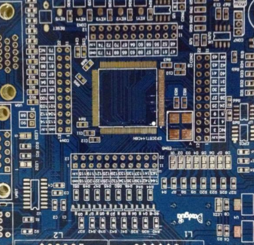
Circuit board

3. Glass fiber PCB base plate
Sometimes, epoxy board, glass fiber board, FR4, fiber board, etc. are added. It uses epoxy resin as the adhesive and glass fiber cloth as the reinforcement material. The working temperature of the circuit board is very high and is not affected by environmental factors. This kind of circuit board is commonly used for double-sided printed circuit board. However, its price is relatively expensive compared with composite PCB substrate, and the common thickness is 1.6 mm. This kind of base plate is applicable to various power boards and advanced circuit boards, and is widely used in computers, peripherals and communication equipment.
Three Reasons of Solder Joint Aging in PCBA Process
Failure mode of solder joint
The reliability test operation of PCBA processing solder joints includes reliability test and specific analysis. The purpose of the first level is to evaluate and test the reliability test level of electronic components on integrated circuit chips, and provide data parameters for the reliability design of the entire equipment; On the other hand, it is to improve the reliability testing of solder joints. This requires specific analysis of the failed product, finding the failure mode, and specific analysis of the cause of the failure. The purpose is to improve and optimize the design process, structural parameters, welding process, etc. The failure mode of solder joints is based on the prediction of the cycle life. Analysis is the key and the basis for creating its mathematical analysis model. Next, we will introduce the three failure modes in detail.
1. Solder joint failure caused by welding process
Some objective conditions in the welding process and the subsequent unreasonable cleaning process may lead to solder joint failure. The reliability test status of surface mount solder joints mainly comes from the production installation stage and the operation stage. In the production and installation stages, due to the limitations of equipment conditions (such as pre welding preparation, welding stage and post welding inspection), as well as human errors in the selection of welding specifications, welding failures are often caused, such as faulty welding, solder short circuit and Manhattan conditions.
On the other hand, in the application stage, due to the inevitable collision and vibration, it will also cause mechanical damage to the solder joints. Bear thermal mechanical stress. When the temperature difference is too large, the ceramic and glass parts of electronic components will cause stress cracks. Stress crack is an objective condition that endangers the long-term reliability test of solder joints.
At the same time, in the installation stage of thick film and thin film hybrid circuits (including chip capacitors), gold and silver corrosion usually occurs. This is because the tin in the welding materials and the gold and silver in the gold or silver plated pins will produce chemicals, which in turn will reduce the reliability test of the solder joints. Excessive ultrasonic cleaning may also be harmful to the reliability test of solder joints.
2. Aging failure
When the molten solder contacts the clean substrate, intermetallic compounds (intermetallic compounds) are formed at the interface. In the aging stage, the microstructure of the solder joint will be coarsened, and the IMC at the interface will continue to grow. The failure of solder joint depends partly on the growth dynamics of IMC layer Although the intermetallic chemicals on the interface are a sign of good welding, with the increase of its thickness in the stage of putting into use, it will lead to microcracks or even fractures in the solder joints
When its thickness exceeds a critical point, the intermetallic chemicals will show brittleness. In view of the mismatch of thermal expansion among various data constituting the solder joint, the solder joint will experience periodic strain in the stage of putting into use. When the variable is large enough, it will cause failure. The research shows that adding trace rare earth element lanthanum to Sn60/Pb40 solder alloy will reduce the thickness of metal chemicals, thus increasing the thermal fatigue life of solder joints by two times, and significantly improving the reliability test of surface mount solder joints.
3. Fault caused by hot loop
When the electronic components are put into use, the periodic disconnection of the power circuit and the periodic change of the working temperature will make the solder joints subject to the temperature cycling process Thermal expansion mismatch between package materials will lead to stress and strain in solder joints If it is mounted on the surface, the thermal expansion coefficient of A1203 ceramic is 6 times; 10-6 ℃ - 1, while the thermal expansion coefficient of epoxy resin/glass fiber substrate is 15 times; 10-6 ℃ - 1. When the temperature changes, the solder joint will bear the corresponding stress and strain Generally, the strain of solder joint is 1% - 20% During THT, the flexible pins of electronic components will absorb most of the strains caused by thermal mismatch, and the solder joints will bear little strain When mounting on the inner surface, the strain is basically borne by the solder joint, which will lead to the initiation and propagation of cracks in the solder joint, and finally failure
The above is the explanation given by the editor of pcb circuit board company.
If you want to know more about PCBA, you can go to our company's home page to learn about it.
In addition, our company also sells various circuit boards,
High frequency circuit board and SMT chip are waiting for your presence again.


Just upload Gerber files, BOM files and design files, and the KINGFORD team will provide a complete quotation within 24h.