
Professional PCB manufacturing and assembly
Building 6, Zone 3, Yuekang Road,Bao'an District, Shenzhen, China
+86-13410863085Mon.-Sat.08:00-20:00

Radio frequency (RF) and microwave PCBs are popular circuit boards that require specific design and layout considerations. In this guide, learn what makes up a successful RF/Microwave PCB project, including design considerations, material selection, integrated components, and more.

What are RF and Microwave PCBs?
Transmission Lines and Impedance
integrated components
Layout techniques and strategies
Materials and Board Stackups Set
Skin effect and loss tangent
shielding and shielding
PCB Materials, Manufacturing and Assembly
What are RF and Microwave PCBs?
RF and microwave PCBs operate on signals in the megahertz to gigahertz frequency range (very low to very high frequencies), which are commonly used in communications ranging from cell phones to military radars. RF and microwave PCBs are one and the same when it comes to layout, fabrication, and assembly guidelines.
Transmission Lines and Impedance
A transmission line is a wire or conductor that transmits energy from one point to another. They are copper structures that transmit electrical signals through the PCB without interruption or noise, and prevent electromagnetic interference (EMI).
There are many types of transmission lines, including:
microstrip
stripline
Surface microstrip (copper traces will run on the surface)
edge-to-face microstrip
Edge-to-Symmetric Stripline
Embedded Microstrip
Striplines are usually embedded, while microstrips are located on the surface. Coplanarity is also another type of transmission line.
All structures of a transmission line will carry impedance.
Integrated components
The exact components will vary depending on the specific PCB, but the following list details the important components that are commonly found in RF/Microwave PCB designs:
amplifier
bluetooth circuit
antenna
Inductor
capacitor
Resistor
filter
coupler
Layout techniques and strategies
You need to know what the impedance is through the transmission line, which is also directly related to the PCB material you choose. An engineer will help determine which type of transmission line is required.
The layout of an RF/Microwave PCB is usually a transmission line on top, copper traces followed by a dielectric material. The second layer is the ground or power plane. All of these directly affect the impedance of the transmission line, the width of the copper traces, and the height of the material on the board.
Noise is one of the most important issues in RF/microwave layouts. These types of PCBs are often made from digital power supplies, which means they can be noisy. It is important to isolate the RF portion of the circuit to avoid such interference. In some cases, you can protect your circuit from space noise; other times you need a grounded barrier or shield around the circuit.
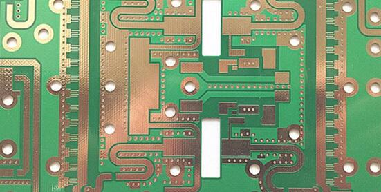
Materials and Board Stackups
RF and microwave PCBs are often fabricated using advanced composite materials with very specific dielectric constant (Er), loss tangent and coefficient of thermal expansion (CTE) properties.
High frequency circuit materials with low stable Er and loss tangent allow high speed signals to pass through the PCB with less impedance than standard FR-4 PCB materials. These materials can be mixed in the same stack for optimum performance and economy.
It is important to consider impedance calculations, which are closely related to material selection. Two-layer boards are relatively simple, but multilayer PCBs can be more challenging. For example, in an RF/Microwave PCB stackup, the transmission lines and ground planes must be adjacent to each other. If they are two layers apart from each other, the software the engineers use will help develop the correct stackup to determine the height and weight of all layers.
Some materials are more suitable for RF/Microwave PCBs than others, but it depends on the frequency. For example, Teflon is ideal for high frequency PCBs because of its low loss tangent.
Skin effect and loss tangent
Skin effect refers to the noise picked up on the board due to copper traces. Loss tangent is a measure of dielectric loss caused by electromagnetic energy. High frequency circuit materials with low stable Er and loss tangent allow high speed signals to pass through the PCB with less impedance than standard FR-4 PCB materials.
RF/Microwave PCBs typically use materials with lower loss tangents.
shielding and shielding
The return path on the circuit must be protected or "shielded" from noise. Shielding can refer to physical shielding or placement of components. Adding vias is another consideration that helps avoid noise and interference.
RF/Microwave PCB Materials, Fabrication and Assembly
Kingford's engineers have extensive experience in handling a wide range of materials related to RF and microwave technology, which helps ensure that your order is manufacturable while being produced on time and on budget. We can provide custom RF and microwave PCB fabrication within 24 hours - all you need to do is request it. In addition, all design, fabrication and assembly can be done at the Kingford factory with no outsourcing.
If you have any questions or would like to learn more about RF/Microwave PCBs, please contact us or request a quote.
What are microvias in PCB design?
Jun 20,2022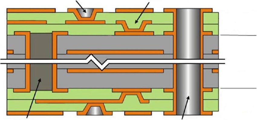


Just upload Gerber files, BOM files and design files, and the KINGFORD team will provide a complete quotation within 24h.