
Professional PCB manufacturing and assembly
Building 6, Zone 3, Yuekang Road,Bao'an District, Shenzhen, China
+86-13410863085Mon.-Sat.08:00-20:00

Once you understand exactly what you want from your pcb prototype and have accumulated the required information, you can begin the pcb prototyping process. An experienced PCB company may support you in this process. Choose a business that offers responsive customer support and helpful tools to make the process as smooth as possible.
Working with us, kingford offers a complete turnkey solution that may help simplify the process as you don't need to communicate with numerous businesses.
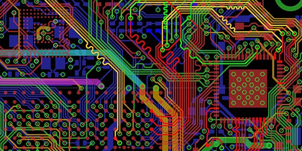
PCB layout
PCB Design/Layout Process Steps
1. Layout
The first step in making a PCB prototype is the design. As mentioned earlier, you can use one of the many PCB design software suites for layout.
2. Schematic
The design describes key recommendations that engineers and manufacturers will use during the manufacturing process. It contains information about the materials, hardware and components used in production and determines the purpose of the board, its own properties and the positioning of the components. Some important aspects of this stage are choosing the ideal panel size and grid.
The design is part of the first design phase. When the designers have completed their initial assessment, they will conduct an initial inspection of possible deficiencies and fix any that arise. You can then run simulations using technical PCB layout tools to ensure the board is functioning properly and function as a more comprehensive layout test. The designer then converts the digital design into a so-called netlist, which explains the interconnectivity of these contained elements.
Frequent design rule checks are required during the design process. This strategy allows you to solve problems and achieve a more efficient design process.
3. Bill of Materials
Next you need a BOM (Bill of Materials). Here is a list of all the components and materials needed to create and information about them. If you're relying on the manufacturer to provide your components, that's really the record they use to make sure you get the right components.
The BOM contains key information for each component, such as:
(1) Quantity: The number of components required.
(2) Reference Designator: A code used to identify body parts.
(3) Value: The specification of each component described in the correct unit, such as Ohms or Farads.
(4) Footprint: The positioning of each part on the PCB board.
(5) Manufacturer's number: The complete component description of the manufacturer's part number should be clear.
After completing the BOM and schematics, design engineers and part engineers will evaluate records and collect important components. Parts engineers are responsible for selecting components that fit the layout and meet customer price and size requirements.
4. Routing
Then you have to design the navigation, with hints, you can use every component that connects this PCB. Different factors come into play when preparing for routing, such as battery level, signal noise generation, and sound sensitivity.
Many PCB design software applications use the netlist you have developed to program the routing. Many of these applications can automatically figure out the best path based on the number of accessible layers and other aspects. This process can sometimes take some time - especially for larger boards or boards with a large number of components.
5. Check
You'll want to periodically check your layout for nearly all performance issues along the way, but before you get to the manufacturing stage, do you do a final full inspection to evaluate every component of your layout for possible issues.
Common issues to look out for include thermal issues such as heating stains. Your layout should keep the planks at a constant temperature. Some design features such as the presence of thermal channels, varying aluminum thicknesses, sizeable PCB dimensions and the number of PCB prototype layers can cause hot spots and inconsistent temperatures.
In addition to some thermal checks, you will also need to run design rule checks, layout and schematic (LVS) tests, electrical rules checks (ERC), and antenna tests. Many producers also perform other assessments for better assurance.
After completing the test, you can send your layout to some PCB manufacturers for PCB fabrication, and you should consider whether their capabilities meet your requirements.
PCB manufacturer
PCB Prototyping Services
Before buying a complete printed circuit board for your job, you need to be sure that your layout is flawless. To do this cost-effectively, you need to create a pcb prototype of your board - a little stripe of your layout to check its performance.
However, you don't need to waste time on the pcb prototyping process. That's why you must use a PCB manufacturing company like KingFord to help you quickly get accurate, cost-effective pcb prototypes. Once you are satisfied with your pcb prototype, we can even complete your entire production run with the exact same quality and efficacy.
Another way to help your pcb prototyping process run smoothly is to identify what it involves so you know what to expect and can easily provide basic information. So, what exactly is involved in pcb prototyping?
Advantages of PCB Prototyping
We recommend that you produce a pcb prototype before purchasing a full production run of a new pcb prototype layout. We make sure our prototype PCB support is user friendly and fast so you can easily check your board. Here's what pcb prototyping allows you to do:
(1) Detect design flaws early in the manufacturing process, before you spend a lot of money
(2) Cost-effectively test multiple layouts
(3) Get a real understanding of how your board will work
Leading PCB Prototyping
Before starting your PCB prototyping process, make sure pcbprototyping is a good fit for your requirements. While it's good for many jobs, it's not essential for every job. If you choose to prototype a pcb, you will need some simple details about your work to get started.
Determine if you need a pcb prototype: Prototypes are best when you want to check the layout or do a good job of checking your PCB.
Whenever you use a factory for a new job, you should use a prototype. If you've successfully produced digital products with this board, you probably don't need a pcb prototype. However, if you create any design modifications or produce a brand new PCB prototype or merchandise, you will need to purchase a pcb prototype.
For our rapid PCB prototyping services, we can fulfill orders of 5 to 100 units and extend build time by 4 to 5 business days.
Organize your PCB prototyping process
To submit your pcb prototyping design or get a quote for a PCB prototyping solution, you should prepare some information about your design. Generally, more information is better - this can get you the results you want. Here is some information to include when submitting a design to a manufacturer:
(1) Number of layers
(2) Plate thickness
(3) Board size
(4) Copper thickness
(5) Minimum trace width/space
(6) Minimum aperture
(7) The smallest ring
(8) Surface treatment
(9) Solder mask color
(11)Silk printing color
(12) Drilling file with NC data
(13) Application list for drilling documents
You can submit your layout files using various software titles. We will convert the document to Gerber RS-274X, which is the perfect file type.
Our PCB Prototyping Capabilities
While going into a full production run may seem more efficient, starting with a pcb prototype may make your manufacturing process more efficient and cost-effective in the future, with improved quality and more predictable performance.
If you use Kingford, you can minimize the extra time required to generate pcb prototypes while maximizing quality and precision. We can imitate your design within three to seven days. We help you reduce costs by enabling prototype orders as low as 5 digits. Of course, we can help you save on development costs by catching design errors and other problems early in the manufacturing process.
We also save time and money because we provide all parts of PCB prototyping, from manufacturing to parts sourcing to meetings. This one-stop shop means you don't need to look for different companies for every area of your program.
At Kingford we have an excellent internal control department and meet all the requirements of ISO900, the benchmark for quality control systems.
Previous:No
RF/Microwave PCB Design and Layout Guidelines
Jun 20,2022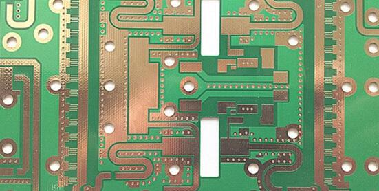


Just upload Gerber files, BOM files and design files, and the KINGFORD team will provide a complete quotation within 24h.