
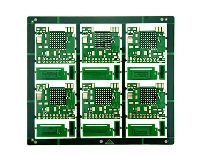
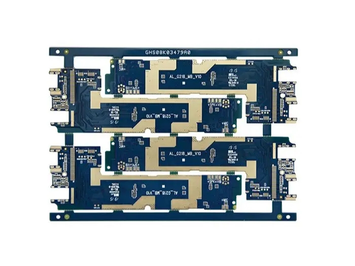
Professional PCB manufacturing and assembly
Building 6, Zone 3, Yuekang Road,Bao'an District, Shenzhen, China
+86-13410863085Mon.-Sat.08:00-20:00


How to optimize PCB design to meet lead-free requirements
At present, lead-free environmental protection is the topic that most PCB manufacturers and PCBA manufacturers talk about and spend great efforts to improve. It is also a technical challenge for manufacturing. As the leader of PCB design, PCB company has also spent a lot of manpower and material resources to carry out some research on PCB design, and has made the following progress: the main optimization design measures include:
1. Improvement of the specification of packaging library
Due to the improvement of lead-free soldering temperature, the influence of device pads on solder joint temperature must be considered when building the library. At the same time, the welding reliability and heat resistance of the device shall be tested to ensure that the size and shape of the pad, the size and shape of the solder resistance, and the relationship between the steel mesh and the pad can meet the optimal welding temperature.
2. Treatment of design methods and details
Avoid the situation of welding and erecting monuments. Therefore, the heating of devices should be considered carefully during design to ensure that each device is heated evenly. Therefore, we have specially developed software to ensure the thermal balance of devices.
3. Selection of surface treatment methods
Different surface treatment methods have different costs and processing difficulties, so there are different surface treatment methods for different products. At the same time, some surface treatment methods have slight differences in packaging or design. For example, when the surface treatment method is OSP, the ICT test point needs to open the steel mesh. For other surface treatment methods, there is no such requirement.

4. Identification description
The plates that need to be lead-free need to be added with identification symbols for subsequent processing manufacturers to identify and handle.
How to Make Copper Foil in FPC
It is well known that copper foil is used as the base material in FPC. However, few people know how it was made. Copper foil is widely used in FPC, but how is it made? The manufacturing methods of copper foil, either calendering annealing or electrolysis, determine their mechanical paradox energy. According to the mechanical properties and applications of copper foil, each kind of copper foil is further divided into different grades. Electrolytic copper foil and forged and rolled copper foil are divided into four grades (Savage. 1992). Generally, electrolytic copper foil is of grade 1 - 4, which is used in rigid printed circuit boards. FPC uses 5 - 8 grades of all electrolytic copper foils and forged and ground copper foils. Typical grades 2, 5, 7 and 8 are used in flexible laminates.
1. Electrolytic copper foil
Electrolytic copper foil is made by electroplating copper ions onto a cylindrical cathode, from which the copper foil is continuously peeled off. The electrolytic copper foil has a columnar grain structure. When the copper foil is bent, the particles are separated, which makes the flexibility and crack resistance of the copper foil smaller than that of the calendered annealed copper foil. The electrolysis process starts with the decomposition of copper from sulfuric acid solution, and the decomposition rate is controlled by temperature and agitation. The shape and mechanical properties of copper foil may be controlled by using different types of additives. Copper solution is continuously injected into the electrolytic cell. Under the action of the current between the anode and cathode of the electrolytic cell, copper ions are separated from the chemical cell to the cathode surface. The cathode is a rotating cylindrical magnetic drum, one part of which is immersed in the solution. When the cathode enters the solution, the copper starts to deposit on the surface of the magnetic drum, and the electroplating is continued until the magnetic drum leaves the solution. When the cathode continues to rotate, the copper foil is stripped from the cathode. The rotating speed of the cathode drum determines the thickness of the copper foil. The electrolytic process can produce copper foil of many thicknesses and widths. The original copper foil products, whether forged or rolled or electrolyzed, also need to be processed in three processing stages. 1) Combined (fixed) treatment; This treatment usually includes the treatment of metal copper/copper oxide, which increases the surface area of copper and provides better wettability for adhesives or resins. 2) Heat resistance treatment; This treatment enables the copper clad laminate to withstand the high temperature environment during PCB manufacturing. 3) Stability treatment; This treatment, also known as passivation or oxidation resistance, is applied to both sides of copper to prevent oxidation and coloring. All stabilization treatments are based on aluminum alloys, and some manufacturers combine nickel, zinc, and other metals with lead. After treatment, the copper coil is cut to the required width, and the cut core is wrapped with plastic film to prevent oxidation. The ductility of copper foil is as follows: 1) electrolytic copper foil: 4% - 40% extension. 2) Calendered annealed copper foil: 20% - 45% extension. Copper foil is usually covered with a film made from polyimide or liquid polymer banyan solution. After this treatment, the conductor film can protect the copper from corrosive environment and solder pollution for a long time.
2. Calendered annealed copper foil
To make calendered annealed copper foil, first heat the copper chain, and then send them to a series of rollers to reduce them to copper foil of specified thickness. The rotation produces the particle structure in the copper foil, which looks like the lapped horizontal plane. Under the action of pressure and temperature, copper particles with different sizes interact with each other, which is the performance of copper foil, such as ductility and hardness, and also produces a smooth surface. Compared with electrolytic copper foil, the copper foil produced by this production process can withstand greater repeated bending. However, it has the disadvantage of high cost and less selectivity of copper foil thickness and width. Copper foil is usually covered with a film made from polyimide or liquid polymer banyan solution. After this treatment, the conductor film can protect the copper from corrosive environment and solder pollution for a long time.


Just upload Gerber files, BOM files and design files, and the KINGFORD team will provide a complete quotation within 24h.