
Professional PCB manufacturing and assembly
Building 6, Zone 3, Yuekang Road,Bao'an District, Shenzhen, China
+86-13410863085Mon.-Sat.08:00-20:00

Practical High Frequency PCB Design and Wiring Principles
Circuit board manufacturers, circuit board designers and PCBA manufacturers explain practical high-frequency PCB design and wiring principles
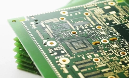
High frequency PCB design and wiring principles
PCB wiring is based on the completion of the basic layout. A certain amount of PCB size should be properly selected during re layout, which can make full use of the middle layer to set shielding, better achieve effective reduction of inductance, near grounding, and reduction of transmission length to reduce signal crosstalk through PCB. All these methods can increase the reliability of high-frequency circuits.
The higher the number of half layers of PCB, the higher the unit cost, and the more complex the manufacturing process. This requires us to select an appropriate number of PCB boards for PCB layout. Use the correct PCB plug-in layout planning and follow the correct routing rules to complete the basic layout. We should also understand the wiring design principle of high-frequency circuit PCB: minimize the logic fan out in the design, and the optimal situation is to carry only one load. Reduce the use of through holes between the output and the receiving end of high-frequency signal transmission within a controllable range to avoid the cross crossing of pin patterns. Pay special attention to the signal line of the clock,. The upper and lower signal lines should be perpendicular to each other to avoid right angle wiring. The load resistance connected at the parallel end shall be as close to the receiving end as possible.
Another key area of high frequency design is the routing of differential pairs, which operate by driving two signal traces in a complementary form. The differential pair provides excellent higher S/N ratio and anti noise capability. In the design of high frequency PCB, the control of PCB characteristic impedance and the design of topology under multi load directly determine the success or failure of the product. Take the chrysanthemum chain topology as an example, which is generally used in the case of single digit MHz. It is recommended to use the star symmetric structure at the back end in the wiring design of high-frequency PCB.
PCB design of high frequency circuit is a complex process, involving many factors, which may directly affect the working performance of high frequency circuit. Therefore, designers need to constantly research and explore in practical work, accumulate experience, and combine new EDA technology to design high-performance high-frequency circuit PCB.
PCB manufacturers, PCB designers, and PCBA manufacturers will explain practical high-frequency PCB design and wiring principles.

Treatment of waste PCB
Nov 12,2022


Just upload Gerber files, BOM files and design files, and the KINGFORD team will provide a complete quotation within 24h.