
Professional PCB manufacturing and assembly
Building 6, Zone 3, Yuekang Road,Bao'an District, Shenzhen, China
+86-13410863085Mon.-Sat.08:00-20:00


What is the specific process of SMT placement?
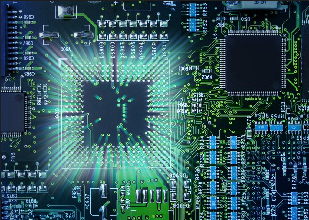
SMT is a surface mounting technology, which is very common in various manufacturing and processing industries. SMT mounting processing is based on PCB board. First, solder paste is printed on the bonding pad of bare PCB board, and then the components are pasted on the bonding pad of PCB board with a mounting machine, and then PCB boards are flowed into reflow soldering for welding. SMT mounting production is a series of processes to paste components on bare PCB board.

What are the specific processes of SMT placement?
The basic elements of SMT mounting process: silk screen, inspection, mounting, reflow welding, cleaning, inspection and maintenance.
1. Silk screen printing: you need to play with the steel mesh and print the solder paste on the PCB pad to prepare for the next step of component welding.
2. Inspection: check the quality of solder paste printing on the printing machine, and then check the tin thickness on the PCB board and the position of solder paste printing. Use the SPI solder paste thickness gauge to check whether the solder paste printing is flat and consistent in thickness, and whether there is any displacement, pointed, etc.
3. SMT mounting: use smt mounting machine to accurately install all components and parts to be assembled on the surface at the fixed position of PCB.
4. Reflow soldering: It is used to melt the solder paste, so that the surface mounted components and PCB board are tightly bonded together. It's behind the mounter.
5. Cleaning: After reflow soldering, there will be a lot of dirt and welding residues left on the PCB board, which needs to be cleaned with a cleaner or manually to achieve the goal of cleanliness.
6. Inspection: After the production is completed, it is necessary to check whether there is any problem in PCB welding in machine equipment such as ICT, AOI, magnifying glass, etc. The boards with problems need to be picked out for maintenance.
7. Repair: PCB boards with faults detected need to be tested to find faults for repair and rework. Ensure that the pcba boards produced are normal.


Just upload Gerber files, BOM files and design files, and the KINGFORD team will provide a complete quotation within 24h.