
Professional PCB manufacturing and assembly
Building 6, Zone 3, Yuekang Road,Bao'an District, Shenzhen, China
+86-13410863085Mon.-Sat.08:00-20:00

PCB Layout design experience: key and difficult points in power PCB design
1、 Power circuit
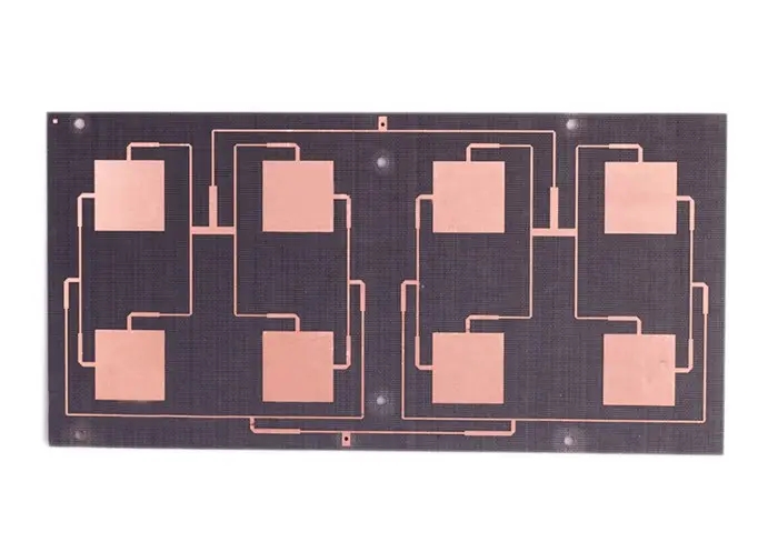
The most important part of the power board is the power circuit. When laying out, you should first know the circuit properties of the distributed power part. In the power supply, the power circuit is mainly divided into di/dt circuit and dv/dt circuit. The two circuits are different when laying out and routing.
The di/dt circuit has a large change in current per unit time, so it is important to pay attention to the smaller loop area of the whole circuit when routing this part of the circuit. It is better to overlap the routing of a loop in different layers, so that the loop area of the circuit is the smallest and the interference generated by itself can be coupled off.
The emphasis of dv/dt circuit is completely different. Because the voltage of this circuit changes greatly in a unit time, it is easy to interfere with the outside world. Therefore, the copper sheet of this circuit cannot be too wide when routing. The copper sheet width should be as small as possible under the condition of meeting the carrying current, the overlapping area of different layers should be as small as possible, and the sensitive signals should be as far away from these routing lines as possible.
2、 Driving part
The area of the whole drive circuit shall be considered first for the line of the drive part, which shall be as small as possible, far away from the interference source and as close as possible to the driven part. For the drive of industrial power components such as MOS tubes, special attention should be paid to the wiring of G and D poles not to run in parallel, because in most cases, the circuit of the D pole part of MOS tubes is a dv/dt circuit, and the G pole is a drive circuit. If it runs in parallel, the drive signal is easy to be interfered, which leads to MOS misoperation.
3、 Sampling signal
Sampling signals such as voltage sampling and current sampling in the power board are also crucial, because the accuracy of these signals is directly related to the control terminal. All these sampled signals should also avoid other signals as far as possible. If conditions permit, these sampled signals can be differential sampled, and they can be given a complete ground plane at the corresponding route.
4、 Disposal of land
Not to mention the importance of the ground, no matter what kind of board it is, it is very important to deal with the ground. The ground in the power board is relatively complex, because the ground with large current in the power part and the ground with small current in the control part are common ground in many cases, so the treatment of these places is very important. In my experience, the key to deal with these places is to select a correct single point connection node. Because each power supply is designed differently, the selection of this single point connection point is also different, In small power photovoltaic inverter, I usually choose a ground pin of the BUS capacitor. In frequency converter, I usually lead a relatively thick wire from the ground pin of a capacitor in the large current to the ground pin of the capacitor at the input end of the switching power supply, and then lead from this ground pin to the ground plane of the small current coming out behind the switching power supply, as well as some other places, such as the ground of the crystal oscillator, the ground of the sampling, etc, The design rules of each company are different, and the way to go is also different. There are also many materials to be processed online.
5、 Safety regulations
Safety regulations are indispensable in the design of power supply products. The requirements of safety regulations in different countries and regions are also different. The pollution level and altitude of the application environment will have a greater impact on the distance that safety regulations should pay attention to. So we must be clear about these factors at the beginning of the design. If there is a safety engineer, they can be asked to provide more professional creepage and clearance distances, In the actual PCBLayout, we should pay special attention to the areas where the metal components are located on the PCB, such as the fuse. Its two ends are metal and its middle is nonmetal. If there is no base, the metal at both ends of the fuse will contact the PCB. The surface wiring around all fuses should avoid these metal areas.
6、 Heat dissipation
For those systems with high power, heat dissipation is also crucial. In general, it is necessary to coordinate with the structure. Before design, it is necessary to understand the heat dissipation mode of the overall structure, which is natural cooling, air cooling or water cooling. Air cooling is divided into air suction and air blowing, which will have a greater impact on the layout.
7、 Electromagnetic compatibility (EMC)
The main thing is that the wiring width of some power parts should not change suddenly. If it is necessary to turn, the turning places should also be as flat as possible without changing suddenly. In addition, sometimes there will be large currents, small currents, and some of the sampled signals share a network, but they should not share a circuit when routing freely. It is better to walk separately.
PCB manufacturers, PCB designers and PCBA manufacturers will explain their PCB Layout design experience: the key and difficult points of power PCB design.


Just upload Gerber files, BOM files and design files, and the KINGFORD team will provide a complete quotation within 24h.