
Professional PCB manufacturing and assembly
Building 6, Zone 3, Yuekang Road,Bao'an District, Shenzhen, China
+86-13410863085Mon.-Sat.08:00-20:00

Pcb design decoupling capacitor and via design, noise and electromagnetic interference
1. Decoupling capacitor configuration
One of the common ways of PCB design is to configure appropriate decoupling capacitors in each key part of the PCB. The general configuration principle of decoupling capacitor is:
(1) The power input terminal is connected with 10~100uf electrolytic capacitor. If possible, it is better to connect the cable above 100uF.
(2) In principle, each integrated circuit chip should be equipped with a ceramic chip capacitor of 0.01uf-0.1uf. If the gap between printed boards is insufficient, a capacitor of 1-10pF can be arranged every 4-8 chips.
(3) For devices with weak noise resistance and large power supply change during shutdown, such as RAM and ROM memory devices, decoupling capacitors should be directly connected between the power line and ground wire of the chip.
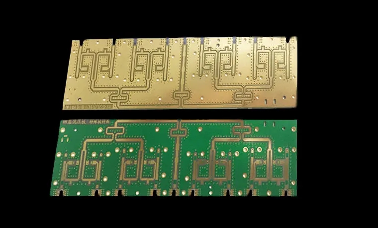
2. Through hole design
In high-speed PCB design, seemingly simple vias often bring great negative effects to circuit design. In order to reduce the adverse effects caused by the parasitic effects of vias, we can try our best to
(1) Considering the cost and signal quality, the reasonable size of vias is selected. For example, for the 6-10 layer memory module PCB design, it is better to select 10/20mil (drilling/pad) vias. For some high-density small size boards, you can also try to use 8/18Mil vias. Under the current technical conditions, it is difficult to use smaller vias (when the depth of the hole exceeds 6 times of the drilling diameter, it is impossible to ensure that the hole wall can be uniformly copper plated); For the via of power supply or ground wire, the larger size can be considered to reduce the impedance
(2) The signal wiring on the PCB shall not change layers as much as possible, that is, unnecessary vias shall not be used as much as possible
(3) The pins of power supply and ground shall be punched nearby, and the lead between the via and pin shall be as short as possible
(4) Place some grounded vias near the vias for signal layer change, so as to provide the nearest circuit for the signal. You can even place a large number of redundant grounding vias on the PCB
3. Some experience in reducing noise and electromagnetic interference
(1) If you can use low-speed chips, you don't need high-speed chips. High speed chips are used in key places
(2) The method of stringing a resistance can be used to reduce the jump rate of the upper and lower edges of the control circuit.
(3) Try to provide some form of damping for relays, such as RC setting current damping
(4) Use the clock with the lowest frequency meeting the system requirements.
(5) The clock shall be close to the device using the clock as much as possible. The shell of the quartz crystal oscillator shall be grounded. The clock area shall be circled with a ground wire. The clock wire shall be as short as possible. The wire shall not be routed under the quartz crystal and the noise sensitive device. The clock, bus and chip selection signal shall be far away from the I/O line and connector. The clock line perpendicular to the I/O line has less interference than the parallel I/O line
(6) The unused gate circuit input terminal shall not be suspended, the unused op amp positive input terminal shall be grounded, and the negative input terminal shall be connected to the output terminal.
PCB manufacturers, PCB designers and PCBA manufacturers will explain the decoupling capacitance and via design of pcb design, noise and electromagnetic interference.


Just upload Gerber files, BOM files and design files, and the KINGFORD team will provide a complete quotation within 24h.