
Professional PCB manufacturing and assembly
Building 6, Zone 3, Yuekang Road,Bao'an District, Shenzhen, China
+86-13410863085Mon.-Sat.08:00-20:00

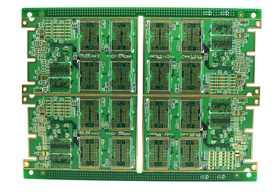
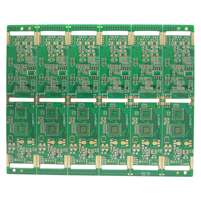
The lamination design of pcb multilayer circuit board
Circuit board manufacturing, circuit board design, PCBA processing manufacturers explain to you the stacking design of four layers of pcb multilayer circuit board manufacturers
As a professional pcb board service provider, we focus on high-precision multilayer boards. Research and development of special plates, pcb proofing and production of small and medium batch plates. Because we are working on medium and high-end boards, we have absolute advantages on multilayer boards. Let's take a look at the laminated design of 4-layer boards in the production of pcb multilayer circuit boards!
From the point of view of signal routing, a good layering strategy should be to place all signal routing on one or several layers, which are close to the power layer or grounding layer. For power supply, when pcb multilayer circuit board is produced, a good layering strategy should be that the power layer is adjacent to the ground plane, and the distance between the power layer and the ground plane should be as short as possible.
There are several potential problems in the design of 4-ply panels. First of all, for the traditional 4-layer plate with a thickness of 62mil, even if the signal layer is in the outer layer and the power supply and ground plane are in the inner layer, the distance between the power supply and ground plane is still too large. If the cost requirement is the first, we can consider the alternatives of two traditional 4-layer boards listed in Table 3-7. These two schemes can improve the performance of EMI suppression, but they are only applicable to the situations where the density of components on the board is low enough and there is enough area around the components (to place the required power supply copper clad layer).
The first is the preferred solution. The outer layer of PCB is the grounding layer, and the middle two layers are the signal/power layer. The power supply on the signal layer is routed with a wide wire, which can make the path impedance of the power supply current low and the impedance of the signal path low. From the perspective of EMI control, this is the best 4-layer PCB structure available.
The outer layer of the second scheme uses power and ground, and the middle two layers use signals. Compared with the traditional 4-layer board, the improvement effect of this scheme is smaller, and the interlayer impedance is as poor as that of the traditional 4-layer board.
If the routing impedance is to be controlled, the routing shall be carefully arranged under the power supply and grounding copper clad island in the above stacking scheme. In addition, the copper clad islands on the power supply or ground plane shall be interconnected as much as possible to ensure the connectivity of DC and low-frequency.
PCB manufacturers, PCB designers, and PCBA manufacturers will explain to you the stacking design of four layers of PCB multilayer circuit board manufacturers.
What is MEGTRON PCB laminate?
Nov 10,2022


Just upload Gerber files, BOM files and design files, and the KINGFORD team will provide a complete quotation within 24h.