
Professional PCB manufacturing and assembly
Building 6, Zone 3, Yuekang Road,Bao'an District, Shenzhen, China
+86-13410863085Mon.-Sat.08:00-20:00


High speed printed circuit board wiring practice guide
PCB routing plays a key role in high-speed circuits, but it is usually one of several steps in circuit design Although a good schematic diagram cannot guarantee a good connection, a good connection starts with a good schematic diagram Please consider carefully when drawing the schematic diagram. You must consider the signal flow of the whole circuit If there is a normal stable signal flow from left to right in the schematic diagram, then there should be the same good signal flow PCB board Provide as much useful information as possible on the diagram Because sometimes the circuit design engineer is absent, the customer will ask us to help solve the circuit problem. The designers, technical personnel and engineers engaged in this work will be very grateful, including us In addition to the universal reference identifier, what other information should be provided in the schematic diagram for power consumption and error tolerance? The following are some suggestions for converting a general schematic to a first level schematic Add waveform, mechanical information of shell, length of printing line and blank area; Indicate which components need to be placed on the PCB; Provides adjustment information, component value range, heat dissipation information, control impedance printed wiring, comments, and circuit overview If you do not design the wiring yourself, make sure you have enough time to carefully check the design of the wiring personnel
PCB board

At this point, a small precaution is better than a hundred times remedy Don't expect the operator to understand your ideas Your comments and guidance are important early in the cabling design process The more information you can provide, the more you intervene in the whole wiring process, the better PCB you will get Set a tentative completion point for the routing design engineer to quickly check the routing progress you want This "closed loop" method can prevent wiring from going astray, thus reducing the possibility of rework The instructions to be provided to the wiring engineer include: a brief description of the circuit function, a schematic diagram of the PCB board instructing the input and output positions, PCB stacking information (for example, how thick and how many layers this board has, and detailed information about each signal layer and ground plane - power consumption, ground wire, analog signal, digital signal and RF signal); which signals are required for each layer; require the placement of important components; the exact location of bypass components; which printed lines are important; which lines need to control impedance printing Lines; which lines need to match the length; the size of the components; which printed lines need to be far away from each other; which lines need to be far away (or close) to each other; which components need to be far away (or close) to each other; Which components need to be placed on the PCB Never complain about too much information to others? Is it too much? no Just like in a PCB, position decides everything The location of the circuit on the PCB, the installation location of its specific circuit components, and what other adjacent circuits are all very important
Usually, the positions of input, output and power supply are predetermined, but the circuits between them need to "exert their creativity". This is why paying attention to cabling details can yield huge returns. From the position of key components, consider the specific circuit and the entire PCB. Specifying the location of key components and signal paths from the start helps ensure that the design meets the intended operational objectives. Getting the right design can reduce the cost and pressure, and shorten the development cycle. In the PCB design process including high-speed operational amplifiers or other high-speed circuits, bypassing the power supply of the amplifier power supply to reduce noise is a very important aspect. There are two common ways to bypass high-speed operational amplifiers. Grounding of power supply terminal: This method is effective in most cases. Multiple parallel capacitors are used to directly ground the power supply pin of the operational amplifier. Generally speaking, two parallel capacitors are sufficient, but adding parallel capacitors may bring benefits to some circuits. The parallel connection of capacitors with different capacitance values helps to ensure that only very low AC impedance can be seen on the power supply pin in the broadband. This is particularly important for op amp power rejection ratio attenuation frequencies. This capacitor helps compensate for the PSR reduction of the amplifier. Maintaining a low impedance ground path over many octave ranges will help ensure that harmful noise does not enter the op amp. Figure 1 shows the advantages of using multiple capacitors in parallel. At low frequencies, large capacitors provide a low impedance grounding path. But once the frequency reaches its resonant frequency, the capacitance of the capacitor will weaken and inductance will gradually appear. This is why it is important to use multiple capacitors: when the frequency response of one capacitor starts to decline, the frequency response of the other capacitor starts to work, and it can maintain very low AC impedance in many 10 octave ranges. Start directly from the power supply pin of the operational amplifier; Capacitors with capacitance values and physical dimensions shall be placed on the same side of the PCB as the operational amplifier and as close to the amplifier as possible. The grounding terminal of capacitor shall be directly connected to the ground plane with short pin or printed wire. The ground connection shall be as close to the load terminal of the amplifier as possible to reduce the interference between the power terminal and the ground terminal. Repeat this process for the capacitor with the next maximum capacitance. The capacitor has a very low series inductance and excellent high frequency efficiency with a housing size of 0508 of 0.01. Power to power: Another configuration method uses one or more bypass capacitors to connect to the positive and negative power terminals of the operational amplifier. This method is usually used when it is difficult to include four capacitors in the circuit. The disadvantage is that the size of the capacitor shell may be increased, because the voltage at both ends of the capacitor is twice the voltage value in the single power bypass method. The new voltage requires the rated breakdown voltage of the new equipment, that is, the size of the new enclosure. However, this method can improve power spectral ratio and distortion efficiency. As each circuit and wiring is different, the configuration, quantity and capacitance value of capacitors shall be determined according to the requirements of the actual circuit. The so-called parasitic effects are small faults that sneak into PCB and cause serious circuit damage, headache and unexplained causes. They are parasitic capacitors and inductors that penetrate into high-speed circuits. The utility model comprises a parasitic inductor formed by a package pin and a long track; Parasitic capacitance formed from pad to ground, pad to power plane and pad to track; Interactions between vias, and many other possible parasitic effects. In high-speed circuits, smaller values will affect the efficiency of the circuit. Sometimes dozens of Pifaras are enough. Related example: If there is only 1 pF additional parasitic capacitance at the inverting input, it will cause a spike of nearly 2 dB in the frequency domain. If the parasitic capacitance is large enough, it will cause instability and oscillation of the circuit. Strip inductance is another parasitic effect to be considered. This is caused by too long printing line or lack of ground plane.
Printed circuit board
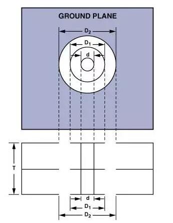
Î µ r represents PCB cloth T represents the thickness of PCB D1 indicates the pad diameter around the through hole D2 is the diameter of the isolation hole in the ground plane All dimensions are organized in centimeters 0 The 157 cm thick PCB can add 1 parasitic inductance 2 nH and 0 parasitic capacitance 5 pF; This is the reason why we need to be alert when wiring PCB board, parasitic effects The ground plane, as a common reference voltage, can discriminate heat and reduce parasitic capacitance (but it also increases parasitic capacitance) Although the use of ground plane has many advantages, it must be implemented with care, because it has some restrictions on what can and cannot be done Ideally, one layer of PCB should be used exclusively as the ground plane This will produce results when the entire plane is not destroyed Do not misappropriate the ground area in the special layer to connect to other signals Because the ground plane can eliminate the magnetic field between the conductor and the ground plane, the inductance of the printed circuit can be reduced If an area of the ground plane is damaged, the printed wiring above or below the ground plane will introduce unexpected parasitic inductance Because the ground plane usually has a large surface area and cross section area, the resistance of the ground plane remains at a value In the low frequency band, the current will choose the resistance path, but in the high frequency band, the current will choose the impedance path However, there are exceptions, sometimes small ground planes are better If the ground plane is moved away from the input or output pads, the high-speed operational amplifier will work better Because parasitic capacitance is introduced on the ground plane of the input terminal, the input capacitance of the operational amplifier is increased, and the phase margin is reduced, resulting in instability As discussed in the Parasitic Effects section, a 1 pF capacitance at the input of the operational amplifier can cause a very noticeable spike Capacitive loads at the output, including parasitic capacitive loads, can cause poles in the reverberation loop This reduces the phase margin and causes the circuit to become unstable If possible, analog and digital circuits, including their respective ground plane and ground plane, should be separated A fast rising edge may cause a small current fault to flow into the ground plane The noise caused by these fast current spikes will destroy the analog efficiency Analog grounding and digital grounding shall be connected to the common grounding point to reduce the digital and analog grounding current and noise of the loop In the high-frequency range, a phenomenon called "skin effect" must be considered The skin effect causes the current to flow on the outer surface of the conductor, making the cross-section of the conductor narrower, thus adding a DC resistance Although skin effect is beyond the scope of this paper, here is a good approximation formula for the skin depth in the copper wire (in cm, low sensitivity electroplating metal helps to reduce skin effect. Wiring and mask, there are various analog and digital signals on PCB, including high to low voltage or current, from DC to GHz frequency range. It is difficult to ensure that these signals do not interfere with each other
The inductive coupling can be reduced by reducing the length of long parallel wires in the same circuit Reducing the length of long traces in adjacent layers can prevent capacitive coupling Signal traces requiring high isolation should be located on different layers. If they cannot be completely isolated, they should be located on orthogonal traces, and then the ground plane should be placed between them Orthogonal wiring can reduce capacitive coupling, and the ground wire will form an electrical mask This method can be used to form a controlled impedance printed circuit High frequency signals usually flow on the control impedance print line That is, the printed circuit maintains the characteristic impedance, such as 50 Ω) Two common control impedance printed lines, microstrip line 4 and stripline 5, can achieve similar effects, but the implementation methods are different H represents the distance from the ground plane to the signal track, W represents the width of the track, and T represents the thickness of the track; All dimensions are organized in mils Î µ r represents PCB cloth The strip control impedance printed wire uses two layers of ground plane, in which the signal printing wire is clamped This method uses more lines, requires more PCB layers, is sensitive to changes in dielectric thickness, and has higher costs. It is usually only used in applications with higher requirements Advanced PCB layout is very important for successful operational amplifier circuit design, especially for high-speed circuits Good schematic diagram is the basis of good wiring; Close cooperation between circuit design engineers and wiring design engineers is essential, especially the location of components and wiring Issues to be considered include bypassing the power supply, reducing parasitic effects, using ground plane, the impact of opamp packaging, and PCB wiring and masking methods
Key points of LVDS signal design on PCB
Nov 09,2022


Just upload Gerber files, BOM files and design files, and the KINGFORD team will provide a complete quotation within 24h.