
Professional PCB manufacturing and assembly
Building 6, Zone 3, Yuekang Road,Bao'an District, Shenzhen, China
+86-13410863085Mon.-Sat.08:00-20:00

Several problems in wearable PCB design
Due to the small size of PCB, there is almost no ready-made PCB standard for the growing wearable Internet of Things market Before these standards are introduced, we must rely on the knowledge and manufacturing experience learned in board level development and think about how to apply them to unique emerging challenges There are three aspects that need our special attention They are circuit board surface data, RF/microwave design and RF transmission lines
PCB board cloth
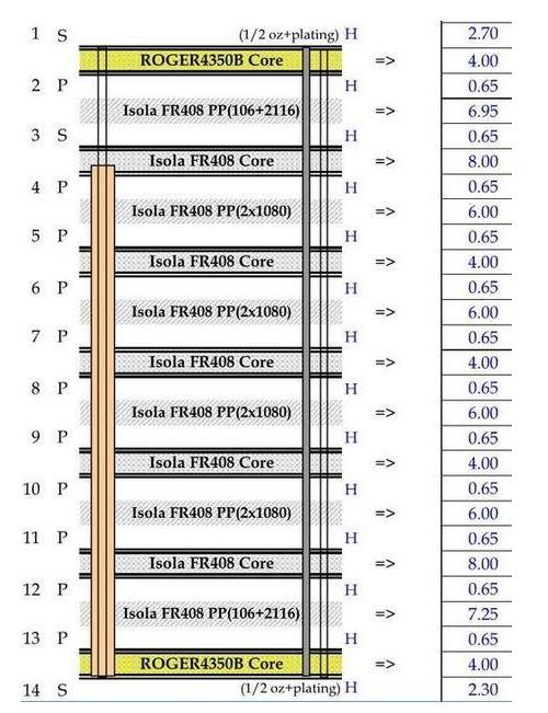
PCB usually consists of laminate, which may be made of fiber reinforced epoxy resin (FR4), polyimide or Rogers information or other laminated information The insulating material between different layers is called prepreg
PCB board
Several key points that should be paid attention to in construction: wearable PCB design
Wearable devices require high reliability. When are PCB designs faced with the choice of using FR4 (a cost effective PCB manufacturing material) or more advanced and more expensive materials If the wearable PCB application requires high-speed and high-frequency data, FR4 may not be the option The dielectric constant (Dk) of FR4 is 4.5, the dielectric constant of more advanced Rogers 4003 series data is 3.55, and the dielectric constant of brother series Rogers 4350 is 3.66. The dielectric constant of laminate refers to the ratio of capacitance or energy between a pair of conductors near the laminate and that between a pair of conductors in vacuum At high frequencies, the loss is small Therefore, Roger 4350 with a dielectric constant of 3.66 is more suitable for higher frequency applications than FR4 with a dielectric constant of 4. 5 Under normal conditions, the number of PCB layers of wearable devices varies from 4 to 8 The principle of layered structure is that if it is an 8-layer PCB board, it should be able to provide enough grounding and power layers and clamp the wiring layer With this kind of pipe, the ripple effect in crosstalk can be maintained and electromagnetic interference (EMI) can be significantly reduced In the design phase of circuit board layout, the floor plan usually places a large ground floor near the distribution floor This can form a very low ripple effect, and the system noise can be reduced to almost zero This is particularly important for RF subsystems Compared with Rogers data, FR4 has a high dispersion factor (Df), especially at high frequencies For FR4 laminates with higher efficiency, the value of Df is about 0.002, which is an order of magnitude better than ordinary FR4 laminates However, Rogers' stack is only 0.001 or less When FR4 data is used in high frequency applications, the insertion loss will be significantly different Insertion loss is defined as the power loss of signal from point A to point B when FR4 is used, Rogers or other data
Manufacturing problem
Wearable PCB boards need more strict impedance control This is an important factor in wearables Impedance matching can produce clearer signal transmission In the early stage, the standard tolerance of signal transmission track is ± 10% This quota is obviously not good enough for today's high frequency and high-speed circuits The current requirement is ± 7%, and in some cases even ± 5% or less This parameter and other variables will seriously affect the extremely strict impedance control of the manufacturing PCB of these wearable devices, thus limiting the number of enterprises that can manufacture them The dielectric constant tolerance of laminates made from Rogers UHF data is usually kept at ± 2%, and some products can even reach ± 1% On the contrary, the dielectric constant tolerance of FR4 laminate is as high as 10% Therefore, comparing the two data, it can be found that Rogers' insertion loss is particularly low Compared with traditional FR4 data, the transmission loss and insertion loss of Rogers stack are half lower In most cases, cost is a problem However, Rogers can provide relatively low loss HF laminate performance at an acceptable price For commercial applications, Rogers can use epoxy resin based FR4 to make mixed PCB. Some layers use Rogers data and others use FR4. When selecting Rogers stack, frequency is the primary consideration When the frequency exceeds 500MHz, PCB design Rogers tends to select Rogers data, especially RF/microwave circuits, because these data can provide higher efficiency when the upper traces are subject to strict impedance control Compared with FR4 data, Rogers data can also provide lower dielectric loss, and its dielectric constant is stable in a wide frequency range In addition, Rogers data can provide ideal low insertion loss performance for high frequency operation The efficiency of thermal expansion (CTE) of Rogers 4000 series materials has excellent dimensional stability This means that compared with FR4, when the PCB is subjected to cold, hot reflow and extremely hot reflow cycles, the thermal expansion and contraction of the PCB can be kept at the stable limit under higher frequency and higher temperature cycles In the case of mixed stacking, it is easy to mix Rogers and high-performance FR4 together using general manufacturing technology and technology. In this regard, it is relatively easy to achieve high manufacturing yield Rogers stacks do not require a special through-hole preparation process Ordinary FR4 cannot achieve very reliable power efficiency, but high-performance FR4 data do have good reliability characteristics. For example, higher Tg data still has relatively low cost and can be widely used. Simple audio design is suitable for complex microwave applications
RF/microwave design considerations
Portable technology and Bluetooth have paid the way for RF Today's frequency range is becoming more and more dynamic A few years ago, very high frequency (VHF) was defined as 2GHz3GHz But now we can see ultra-high frequency (UHF) applications ranging from 10GHz to 25GHz. Therefore, more attention should be paid to the wiring problems of wearable PCB boards and RF parts. The signals must be separated, and the track generating high-frequency signals must be far away from the ground Other considerations include: provision of bypass screening procedures, sufficient decoupling capacitors, grounding, and design to make the transmission line and return line almost equal The bypass filter can suppress the ripple effect of noise content and crosstalk The decoupling capacitor needs to be placed closer to the device pin carrying the power signal High speed transmission lines and signal circuits need to place a ground plane between the power layer signals to smooth the jitter generated by noise signals At higher signal speeds, small impedance mismatch will lead to unbalanced signal transmission and reception, resulting in distortion Therefore, special attention must be paid to impedance matching problems related to RF signals, because RF signals have high speed and special tolerances RF transmission lines need controlled impedance to transmit RF signals from specific IC substrates to PCB boards These transmission lines can be implemented in the outer layer, top layer and bottom layer, or they can design the ed The methods used in the RF layout process include microstrip lines, suspended striplines, coplanar waveguides, or grounding The microstrip line consists of a fixed length of metal or track and the whole ground plane or part of the ground plane directly below it The characteristic impedance range in general microstrip line structure is 50 Î © To 75 Î ©.
PCB board design in three wearable fields ers need to pay attention to
Suspended stripline is another method of wiring and suppressing noise The line consists of fixed width wiring on the inner layer and large ground plane above and below the central conductor The ground plane is clamped between the power planes. In retrospect, it can provide a very effective grounding effect This is the preferred method for RF signal wiring on wearable devices PCB boards Coplanar waveguides provide better isolation between RF lines and lines that need to go closer The medium consists of a central conductor and a ground plane on both sides or below The method of transmitting RF signal is suspended stripline or coplanar waveguide These two methods can provide better isolation between signals and RF trajectories It is recommended to use the so-called "through-hole fence" on both sides of the coplanar waveguide This method can provide a row of grounding vias on each metal grounding plane of the central conductor There are fences on both sides of the main road in the middle, which provides a shortcut for the return current This method can reduce the noise level related to the high ripple effect of RF signals 4 5 The FR4 data of the prepreg are the same, while the dielectric constant, strip line or offset strip line of the microstrip prepreg are about 3.8 to 3.9. In some equipment using ground plane, the blind hole can be used to improve the decoupling efficiency of the power capacitor and provide a shunt path from the equipment to the ground The shunt path to the ground can shorten the length of the through-hole, which can achieve two purposes: you can not only create a shunt or grounding, but also reduce the transmission distance of the small grounding device, which is an important RF PCB design factor

Line width and copper thickness in PCB design
Nov 09,2022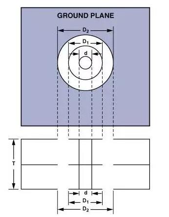


Just upload Gerber files, BOM files and design files, and the KINGFORD team will provide a complete quotation within 24h.