
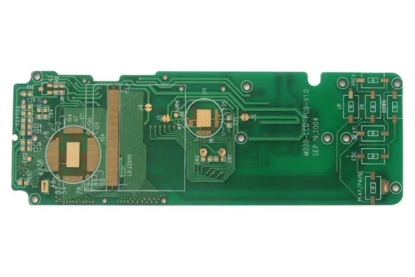
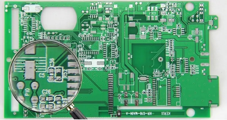
Professional PCB manufacturing and assembly
Building 6, Zone 3, Yuekang Road,Bao'an District, Shenzhen, China
+86-13410863085Mon.-Sat.08:00-20:00

Electronic manufacturer: matters needing attention in power supply PCBA design
With the increasing diversification of the industry, power supply products continue to develop in the direction of high frequency, high efficiency, high density, low voltage and diversification, which leads to greater challenges in the PCBA design of power supply products. What should we pay attention to when designing power PCBA?
First, we should have a reasonable direction
Like input/output, AC/DC, strong/weak signal, high frequency/low frequency, high voltage/low voltage, etc., their trends should be linear or separate, and should not be mixed with each other. The purpose is to prevent mutual interference. The best direction is straight, and the worst direction is circular.
2. Reasonably arrange power filter/decoupling capacitor
Generally, only a few power supply filter/decoupling capacitors are drawn in the schematic diagram, but no indication is given on where they should be connected. In fact, these capacitors are set for switching devices (gate circuits) or other components requiring filtering/decoupling. These capacitors should be arranged as close to these elements as possible, if they are too far away, they will not work. Interestingly, when the power filter/decoupling capacitor layout is reasonable, the problem of grounding point is not so obvious.
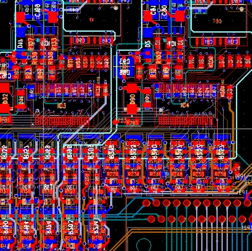
3. Introduction of components and networks
It should be simple to introduce components and networks into the drawn border. However, problems often occur here. Be careful to solve the problems one by one according to the prompted errors. In general, the problems here are as follows: the packaging form of components cannot be found, component network problems, and unused components or pins. These prompted problems can be solved quickly.
4. Pay attention to the size of wire, wire diameter and through hole.
If conditions permit, do not make wide lines thin; High voltage and high frequency lines shall be flat without sharp corners and corners, and shall not turn at right angles. The ground wire should be as wide as possible. It is better to use a large area of copper coating to greatly improve the docking and positioning problem. The pad or through-hole size is too small, or the pad does not match the drilling size. That is to say, after the corrosion in the non wiring area is completed, the thin wires are likely to be corroded too much, or broken, or completely broken. Therefore, the role of copper coating is not only to increase the area of ground wire and anti-interference.
The circuit board manufacturer, circuit board designer and PCBA manufacturer explain the matters that should be paid attention to when designing the power supply PCBA.


Just upload Gerber files, BOM files and design files, and the KINGFORD team will provide a complete quotation within 24h.