
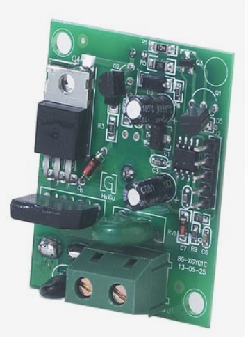
Professional PCB manufacturing and assembly
Building 6, Zone 3, Yuekang Road,Bao'an District, Shenzhen, China
+86-13410863085Mon.-Sat.08:00-20:00

This paper discusses some principles of layout and wiring that should be paid attention to in the process of using PROTEL design software to realize the design of high-speed PCB, and provides some practical and verified high-speed circuit layout and wiring technologies, which improves the reliability and effectiveness of high-speed circuit board design. The results show that the design shortens the product development cycle and enhances the market competitiveness.

1. Problem posing
With the large-scale improvement of the complexity and integration of electronic system design, the clock speed and device rise time become faster and faster. High speed circuit design has become an important part of the design process. In high-speed circuit design, the inductance and capacitance on the circuit board will make the wire equivalent to a transmission line. Incorrect layout of terminal components or wrong wiring of high-speed signals will cause transmission line effect problems, resulting in incorrect data output of the system, abnormal circuit operation or even complete failure. Based on the transmission line model, to sum up, the transmission line will bring adverse effects such as signal reflection, crosstalk, electromagnetic interference, power and ground noise to the circuit design.
In order to design a high-speed PCB that can work reliably, we must give full and careful consideration to the design, solve some unreliable problems that may occur during the layout and routing, shorten the product development cycle, and improve the market competitiveness.
2 Layout design of high frequency system
In PCB design of circuit, layout is an important link. The quality of layout results will directly affect the wiring effect and system reliability, which is the most time-consuming and difficult in the whole PCB design. The complex environment of high frequency PCB makes the layout design of high frequency system difficult to use the theoretical knowledge learned. It requires that the board laying personnel must have rich experience in high-speed PCB manufacturing, so as to avoid detours in the design process and improve the reliability and effectiveness of circuit work. In the process of layout, comprehensive consideration shall be given to mechanical structure, heat dissipation, electromagnetic interference, convenience and aesthetics of future wiring, etc.
3 Wiring of high frequency system
In the high-frequency circuit, the distribution parameters of resistance, capacitance, inductance and mutual inductance of the connecting wire cannot be ignored. From the perspective of anti-interference, reasonable wiring is to try to reduce the line resistance, distributed capacitance and stray inductance in the circuit to minimize the stray magnetic field generated thereby, so that the distributed capacitance, magnetic flux leakage, electromagnetic mutual inductance of the circuit and other interference caused by noise can be suppressed.
The PROTEL design tool has been widely used in China. However, many designers only focus on the "pass rate", and the improvements made to the PROTEL design tool to adapt to the changes in device characteristics have not been used in the design. This not only causes a serious waste of design tool resources, but also makes it difficult to play the excellent performance of many new devices.
The following describes some special functions that PROTEL99 SE tool can provide.
(1) The lead between pins of high-frequency circuit components shall be bent as little as possible. It is better to use full straight line. When bending is required, 45 ° broken line or arc bending can be used to reduce the external transmission and mutual coupling of high-frequency signals. When using PROTEL for wiring, you can select 45 Degrees or Rounded from "Routing Corners" in "Rules" in the "Design" menu, or you can use the shift+space key to quickly switch lines.
(2) The shorter the lead between pins of high-frequency circuit components, the better.
The most effective way for PROTEL 99 to meet the shortest routing is to make routing reservation for some key high-speed networks before automatic routing. Select shortest from Routing Topology in Rules of the Design menu
(3) The lead layer alternation between pins of high-frequency circuit devices shall be as little as possible. That is, the fewer vias used in the component connection process, the better.
One via can bring about 0.5pF distributed capacitance, and reducing the number of via can significantly improve the speed.
(4) For high frequency circuit wiring, pay attention to the "cross interference" (crosstalk) introduced by the distance between signal lines and parallel lines. If parallel distribution cannot be avoided, a large area of "ground" can be arranged on the opposite side of the parallel signal line
To greatly reduce interference. Parallel routing in the same layer is almost unavoidable, but in two adjacent layers, the direction of routing must be perpendicular to each other, which is not difficult to achieve in PROTEL but easy to ignore. In the "RoutingLayers" of "Rules" in the "Design" menu, select Horizontal for Toplayer and Vertical for BottomLayer. In addition, "Polygonplane" is provided in "place"
The function of, namely, polygonal grid copper foil surface. If the polygon is placed, it is taken as a surface of the entire printed circuit board, and the copper coating is connected with the GND of the circuit, which can improve the high-frequency anti-interference ability, and also has greater advantages for heat dissipation, printed board strength, etc.
(5) Measures to enclose signal lines or local units of special importance with ground wires. "Outline selectedobjects" is provided in "Tools". This function can be used to automatically "wrap ground" the selected important signal lines (such as oscillation circuits LT and X1).
(6) In general, the power line and ground line of the circuit should be wider than the signal line. The "Classes" in the "Design" menu can be used to classify the network into power network and signal network. Combining the setting of wiring rules, it is convenient to switch the line width of the power line and signal line.
(7) All kinds of wiring cannot form a loop, nor can the ground wire form a current loop. If a loop circuit is generated, it will cause great interference in the system. The daisy chain wiring method can be used to effectively avoid the formation of loops, branches or stumps during wiring, but it will also lead to the problem of difficult wiring.
(8) According to the data and design of various chips, the current passed by the power line is estimated, and the required wire width is determined. According to the empirical formula, W (line width) ≥ L (mm/A) × I(A)。
According to the current, try to increase the width of the power line and reduce the loop resistance. At the same time, make the direction of power line and ground wire consistent with the direction of data transmission, which helps to enhance the anti noise ability. When necessary, high-frequency choke devices made of copper wire wound ferrite can be added to the power line and ground wire to block the transmission of high-frequency noise.
(9) The wiring width of the same network should be consistent. The change of the line width will lead to uneven characteristic impedance of the line. When the transmission speed is high, reflection will occur, which should be avoided as far as possible in the design. At the same time, increase the line width of parallel lines. When the center distance of lines is not more than 3 times the line width, 70% of the electric fields can not interfere with each other, which is called the 3W principle. This can overcome the influence of distributed capacitance and inductance brought by parallel lines.
4 Design of power line and ground wire
In order to solve the problem of power supply noise and voltage drop caused by line impedance introduced by high-frequency circuit, the reliability of power supply system in high-frequency circuit must be fully considered. There are generally two solutions: one is to use power bus technology for wiring; The second is to use a separate power supply layer. Comparatively speaking, the production process of the latter is more complex and expensive. Therefore, the network type power bus technology can be used for wiring, so that each component belongs to a different circuit, and the current on each bus on the network tends to balance, reducing the voltage drop problem caused by line impedance.
High frequency transmission power is relatively large. Large area copper coating can be used to find the nearest low resistance grounding ground for multi-point grounding. Because the inductive reactance of the grounding lead is proportional to the frequency and length, the common grounding impedance will be increased when the operating frequency is high, which will increase the electromagnetic interference generated by the common grounding impedance, so the length of the ground wire is required to be as short as possible. Minimize the length of the signal line and increase the area of the ground loop.
One or several high-frequency decoupling capacitors are set at the power and ground ends of the chip to provide a nearby high-frequency channel for the transient current of the chip, so that the current cannot pass through the power supply line with a large loop area, thus greatly reducing the noise radiated outward. Single stone capacitive ceramic chip capacitor with good high-frequency signal shall be selected as decoupling capacitor. Use high-capacity tantalum capacitor or polyester capacitor instead of electrolytic capacitor as the energy storage capacitor for circuit charging. Because the distributed inductance of electrolytic capacitor is large, it is invalid for high frequency. When using electrolytic capacitors, they should be used in pairs with decoupling capacitors with good high-frequency characteristics.
5 Other high-speed circuit design technologies
Impedance matching refers to a working state in which the load impedance and the internal impedance of the excitation source match each other to obtain the maximum power output. During high-speed PCB wiring, the impedance of the line is required to be 50 Ω to prevent signal reflection. This is an approximate number. Generally, the coaxial cable baseband is 50 Ω, the frequency band is 75 Ω, and the twisted pair is 100 Ω. It is just an integer, for the convenience of matching. According to the specific circuit analysis, parallel AC termination is adopted. Resistance and capacitance network are used as the termination impedance. The termination resistance R must be less than or equal to the transmission line impedance Z0, and the capacitance C must be greater than 100 pF. 0.1UF multilayer ceramic capacitor is recommended. The capacitor has the function of resistance low frequency and pass high frequency, so the resistance R is not the DC load of the drive source, so this termination mode has no DC power consumption.
Crosstalk refers to the unwanted voltage noise interference on adjacent transmission lines due to electromagnetic coupling when signals propagate on transmission lines. Coupling is divided into capacitive coupling and inductive coupling. Excessive crosstalk may cause false triggering of the circuit, resulting in the system not working properly. According to some characteristics of crosstalk, several main methods for reducing crosstalk can be summarized:
(1) Increase the line spacing, reduce the parallel length, and use the jog method for wiring if necessary.
(2) When the conditions for high-speed signal lines are met, the addition of termination matching can reduce or eliminate reflection, thereby reducing crosstalk.
(3) For microstrip transmission lines and ribbon transmission lines, the crosstalk can be significantly reduced by limiting the routing height above the requirements of the ground plane.
(4) If the wiring space allows, insert a ground wire between the two lines with serious crosstalk, which can play the role of isolation and reduce crosstalk.
Due to the lack of high-speed analysis and simulation guidance in traditional PCB design, the signal quality cannot be guaranteed, and most problems must be found after plate making test. This greatly reduces the design efficiency and improves the cost, which is obviously unfavorable in the fierce market competition. As a result, people in the industry have put forward a new design idea for high-speed PCB design, which has become a "top-down" design method. Through policy analysis and optimization in many aspects, most possible problems have been avoided, a lot of time has been saved, engineering budget has been met, high-quality printed boards have been produced, and tedious and costly testing and error detection have been avoided.
The transmission of digital signals by differential lines is an effective measure to control the factors that damage the integrity of signals in high-speed digital circuits. The differential line on the printed circuit board is equivalent to the differential microwave integrated transmission line pair working in the quasi TEM mode, wherein the differential line on the top or bottom layer of the PCB is equivalent to the coupling microstrip line, and the differential line on the inner layer of the multilayer PCB is equivalent to the wide side coupling stripline. When digital signals are transmitted on the differential line, they are transmitted in odd mode, that is, the phase difference between positive and negative signals is 180 °, and the noise is coupled on a pair of differential lines in a common mode mode. The positive and negative voltages or currents in the receiver are subtracted to obtain signals to eliminate common mode noise. The low voltage amplitude or current driven output of differential line pair meets the requirements of high speed integration and low power consumption.
6 Conclusion
With the continuous development of electronic technology, it is urgent to understand the signal integrity theory, and then guide and verify the design of high-speed PCB. The experience summarized in this paper can help high-speed circuit PCB designers shorten the development cycle, avoid unnecessary detours, and save manpower and material resources. Designers should continue to research and explore in practical work, accumulate experience, and combine new technologies to design high-performance high-speed PCB.


Just upload Gerber files, BOM files and design files, and the KINGFORD team will provide a complete quotation within 24h.