
Professional PCB manufacturing and assembly
Building 6, Zone 3, Yuekang Road,Bao'an District, Shenzhen, China
+86-13410863085Mon.-Sat.08:00-20:00

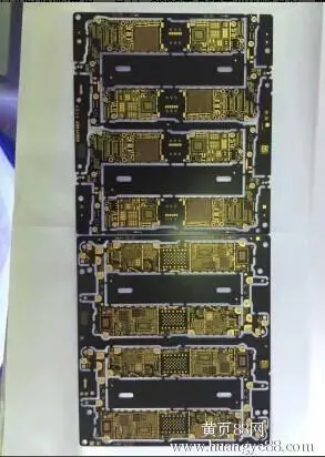
When I first got to know the battery circuit board, I would be scared by each layer of the circuit board. Each layer has its own functions. The division of labor is strict and the content is complex. Let's give you a systematic introduction today!
Circuit board design
As the name implies, the mechanical layer is used for mechanical forming, that is, the appearance of the entire battery circuit board. In fact, when we talk about the mechanical layer, we mean the appearance structure of the entire battery circuit board. It can also be used to set the overall dimensions, data marks, alignment marks, assembly instructions and other mechanical information of the circuit board. This information varies according to the requirements of the design company or the battery PCB manufacturer. In addition, mechanical layers can be connected to other layers for output display.
2. Keep out layer is used to define the area where components and wiring can be effectively placed on the circuit board. Draw a closed area on this layer as the valid area for routing. Cannot automatically lay out and route outside this area. When we lay copper with electrical characteristics, the forbidden wiring layer defines the boundary, that is, after we first define the PCB wiring layer, we cannot lay wires with electrical characteristics outside the boundary of the forbidden wiring layer in the subsequent laying process. It is usually wrong to use forbidden layers as mechanical layers. Therefore, it is recommended that you distinguish them, otherwise the sheet factory will change the attributes for you each time during production.
3. Signal layer: the signal layer is mainly used to lay the wires on the circuit board. It includes Top layer, Bottom layer and 30 MidLayers. The top layer and bottom layer are used to place devices, and the inner layer is used for wiring.
4. Top paste and bottom paste are the steel mesh layers of the top and bottom pads, which are the same size as the pads. This is mainly because we can use these two layers to make the steel mesh when making SMT. We just dig a hole of the size of the pad on the rigid mesh. Then we cover the steel mesh on the battery circuit board, and use a brush with solder paste to brush the solder paste evenly.
5. Top Solder and Bottom Solder are PCB solder mask layers, which prevent the green oil from covering. We often say "window opening". Conventional copper coating or wiring is covered with green oil by default. If we treat the solder mask layer accordingly, it will prevent the green oil from covering and expose the copper.
6. Internal plane layer: This type of layer is only used for multi-layer PCB boards, mainly for arranging power lines and grounding wires. We call it double-layer board, four layer board and six layer board, usually referring to the number of signal layers and internal power/ground layers.
7. Silkscreen layer: The silk screen layer is mainly used to place printing information, such as the outline and annotation of PCB components, various annotation characters, etc.
8. Multi layer: The pads and through-hole on the circuit board need to penetrate the entire circuit board to establish electrical connection with different conductive graphic layers. Therefore, the system has set up an abstract layer - multilayer. Generally, pads and vias must be set on multiple layers. If this layer is closed, pads and vias cannot be displayed.
9. Drill Drawing: The drilling layer provides the drilling information during the manufacturing process of the circuit board (such as the pad, which needs to be drilled through holes).
PCB layout skills and process defect handling
Nov 01,2022


Just upload Gerber files, BOM files and design files, and the KINGFORD team will provide a complete quotation within 24h.