
Professional PCB manufacturing and assembly
Building 6, Zone 3, Yuekang Road,Bao'an District, Shenzhen, China
+86-13410863085Mon.-Sat.08:00-20:00

With the development of economy and science and technology, people put forward higher and higher requirements for electronic products with multi-function, miniaturization, high-density, high-performance and high-quality. Therefore, for PCBA processing industry, high welding quality is the life insurance of electronic products.
Why SMT welding is one of the important links in the assembly process of electronic products. If there is no corresponding SMT welding process quality assurance, then any well-designed electronic equipment will be difficult to achieve the design goals. Therefore, the solder joints shall be strictly checked during welding to prevent unqualified solder joints from causing unqualified electronic products. Next, we will introduce the disadvantages of various electronic SMT welding.
First of all, after the SMT welding operation, in order to make the product have reliable functions, the welding quality should be checked. Welding inspection is generally a visual inspection, not only to inspect the solder joints, but also to check the conditions around the solder joints, such as problems derived from welding. The inspection of wiring and welding of the terminal is to check the welding condition to see whether the insulation skin of the used wire is damaged and whether the terminal is damaged; The bending degree and tightness of the wire hook welded, and whether there are dirty spots in each part. Many of the electronic components found in the electrical function check are damaged due to poor welding.
After all, the welding of electronic products is mainly used for electrical connection. If products with defects in electrical connection have problems, they must be repaired to eliminate their defects.
However, in actual manufacturing, welding defects usually occur, especially in the reflow phase. In fact, the welding problems at this stage are not entirely caused by reflow technology, because SMT welding quality is closely related to the manufacturability of PCB pads, steel mesh design, solderability of components and PCB pads, manufacturing equipment status, and solder quality. The pasting and technical parameters of each link and the operating skills of each worker.
Problems may occur in each link, thus affecting the welding quality of SMT. In this paper, elements that may affect SMT welding quality will be discussed and analyzed to avoid similar problems in actual manufacturing.
BOM preparation
As one of the most important composite materials in SMT, the quality and performance of BOM are directly related to the quality of reflow welding. Specifically, the following aspects must be considered:
1. The component packaging must meet the automatic installation requirements of the installation procedures.
2. Part graphics must meet the requirements of automatic SMT, because it must have standard shapes with high dimensional accuracy.
3. The welding quality of solderable ends of components and PCB pads shall meet the requirements of reflow soldering, and the solderable ends of components and pads shall not be polluted or oxidized. If the weldable ends of components and PCB pads are oxidized, contaminated or wet, some welding defects may occur, such as poor wetting, false soldering, solder beads or cavities. This is especially true for humidity sensor and PCB management. The humidity sensor must be stored in the drying oven after vacuum packaging, and it is necessary to bake before the next manufacturing.
Design for manufacturability of PCB pad
The level of SMT depends on the PCB design quality and is the first factor affecting the surface mounting quality. Based on the statistics from HP, 70% to 80% of manufacturing defects derive from PCB design problems in the selection of substrate materials, conversion component layout, pad and thermal conductive pad design, solder mask design, component packaging type, component method, transmission boundary, through positioning, optical fixing point, EMC (electromagnetic compatibility), etc.
For PCB with correct pad design, even if a little skew occurs during surface mounting, it can be corrected under the effect of surface tension of molten tin, which is called automatic positioning or self correction effect. However, if the PCB pad is not designed correctly, even if the installation position is very accurate, welding defects will still be encountered, such as component position offset and monument. Therefore, the following aspects must be carefully considered in SMT pad design.
1. Symmetry of pads. In order to avoid the position deviation and monument problem after reflow soldering, for chip modules of 0805 and below, the pads at both ends should be symmetrical in terms of pad size, heat absorption and heat dissipation capacity, so as to maintain the balance of melting surface tension. Soldering. If one end is on the large copper foil, it is recommended to use a single wire connection to connect the pads on the large copper foil.
2. Space between pads. In order to ensure that the lapping size between the end of the component or between the pin and the pad is appropriate, when the space between pads is too large or too small, it will often lead to welding defects.
3. The remaining dimensions of the pad must ensure the crescent weld after the end of the component or the overlap between the pin and the pad.
4. The width of pad shall be basically compatible with the width of component end or pin.
5. Do not place through holes on pads. Otherwise, molten tin may flow along the through-hole during reflow soldering, resulting in false soldering and insufficient tin. It may flow to the other side of the board, causing a short circuit.
Solder paste printing
The main purpose of solder paste printing technology is to solve the problem of incompatibility with solder paste printing amount (solder paste filling amount and transfer amount). According to professional statistics, under the condition of correct PCB design, 60% of reworked PCBs are caused by poor solder paste printing. In solder paste printing, three important "S" must be remembered: solder paste, steel mesh and scraper. If selected correctly, excellent printing results can be obtained.
1. Quality of solder paste
As a necessary material for reflow welding, solder paste is a kind of solder paste which is composed of alloy powder and flux (rosin, thinner, stabilizer, etc.) uniformly mixed, in which alloy powder is the key element of solder joint. Flux is the key material to eliminate surface oxidation, improve wettability and ensure the quality of solder paste. In terms of quality, in general, 80% to 90% of the solder paste belongs to metal alloy, accounting for 50% of its volume. Solder paste quality assurance mainly comes from two aspects: storage and application. Solder paste is usually stored between 0 and 10 ℃, or according to the manufacturer's requirements. For its application, the temperature of the SMT workshop must be 25 ℃± 3 ℃ and the humidity must be 50% ± 10%. Moreover, its recovery time must be more than 4 hours, and it must be fully stirred before use, so that its viscosity has excellent printability and demoulding deformation. After the solder paste is coated, the solder paste cover must be placed correctly, and the circuit board coated with solder paste must be reflowed within two hours.
2. Steel mesh design
The key function of the stencil is to evenly coat the solder paste on the PCB pad. Steel screen is indispensable in printing technology, and its quality directly affects the quality of solder paste printing. So far, there are three ways to make steel mesh: chemical etching, laser cutting and electroplating. Mold design cannot be ensured until the following aspects have been fully considered and properly handled.
3. Thickness of steel plate
In order to ensure the quantity of solder paste and welding quality, the surface of the steel mesh must be smooth and flat, and the selection of steel plate thickness should be determined by the component with the minimum spacing between pins.
4. Aperture design
The opening is trapezoidal section and trumpet shaped. Their walls are smooth and free from burrs. Width thickness ratio=hole width/steel mesh thickness (for small spacing QFP, IC); Area ratio=basic area of hole/wall area of hole (for 0201, BGA, CSP parts). c. Anti welding ball processing. The anti solder ball treatment on the steel mesh of the CHIP component 0603 or above can effectively avoid the solder ball after reflow. For components with too large pads, it is recommended to use mesh generation to prevent excessive tin generation. d. Mark. At least 3 MARK points shall be generated on the B side of the steel mesh, and the steel mesh shall be compatible with the MARK on the PCB. In order to increase the printing accuracy, there should be a pair of MARK points with the longest diagonal distance. e。 Printing direction. The printing direction is also a key control point. In the process of determining the printing direction, components with small spacing between them should not be too close to the guide rail. Otherwise, excessive tin may cause bridging.
5. Scraper
The scraper will affect the printing quality to some extent based on its different hardness materials and shapes. Generally, steel scrapers with nickel plating are used, usually 60 ° scrapers. If there is a through-hole assembly, it is recommended to use a 45 ° scraper to increase the tin content on the through-hole assembly.
6. Printing parameters
Printing parameters mainly include scraper speed, scraper pressure, stencil downward release speed, stencil cleaning mode and frequency. The angle between the scraper and the steel mesh does have a restrictive relationship with the viscosity of the solder paste. Therefore, only by correctly controlling these parameters can the printing quality of the solder paste be ensured. In general, the low speed of the scraper results in relatively high printing quality, and the shape of the solder paste may be blurred. In addition, the extremely low speed even reduces the manufacturing efficiency. On the contrary, a high-speed scraper may cause insufficient solder paste filling in the mesh. Too high scraper pressure may lead to insufficient tin, which increases the wear between the scraper and the steel mesh, while extremely low pressure may lead to incomplete solder paste printing. Therefore, when rolling the solder paste normally, the speed should be increased as much as possible. In addition, the scraper pressure should be adjusted to achieve high print quality. The extremely high downward release speed may cause the solder paste to ice or form undesirable phenomena, while the low speed release will affect the manufacturing efficiency. Improper cleaning method and frequency of steel mesh will lead to incomplete cleaning of steel mesh, and continuous tin electrodeposition or insufficient tin in steel mesh will lead to products in narrow space. The extremely high downward release speed may cause the solder paste to ice or form undesirable phenomena, while the low speed release will affect the manufacturing efficiency. Improper cleaning method and frequency of steel mesh will lead to incomplete cleaning of steel mesh, and continuous tin electrodeposition or insufficient tin in steel mesh will lead to products in narrow space. The extremely high downward release speed may cause the solder paste to ice or form undesirable phenomena, while the low speed release will affect the manufacturing efficiency. Improper cleaning method and frequency of steel mesh will lead to incomplete cleaning of steel mesh, and continuous tin electrodeposition or insufficient tin in steel mesh will lead to products in narrow space.
7. Equipment accuracy
In printing products with high density and small space, printing precision and repeated printing precision will affect the stability of solder paste printing.
8. PCB support
PCB support is an important adjustment for solder paste printing. If the PCB lacks effective support or the support is improper, thick solder paste or uneven solder paste should be used. PCB supports shall be arranged flat and evenly to ensure the tightness between the steel mesh and PCB.
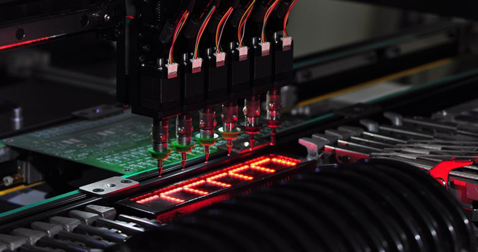
Element installation
The quality of component installation depends on three elements: correct selection of components, accurate placement and appropriate installation pressure. Proper selection of components refers to the fact that components must be compatible with BOM requirements. Correct placement means that the coordinates must be correctly installed, and the accuracy of the installation procedures must ensure the stability of installation and the correct installation of components on the pad. At the same time, attention must be paid to the installation angle to ensure the correct orientation of the components. The proper installation pressure refers to the pressing thickness of the component, and must not be too small or too large. The mounting pressure can be determined by setting the PCB thickness, component package thickness, nozzle mounting machine pressure and adjusting the Z axis of the mounting machine.
Reflow soldering
The welding quality of the solder joint depends on the correct setting of the reflow temperature curve. A good reflow soldering curve requires that all mounting components on the PCB must receive excellent soldering, and the solder joints should have both excellent appearance and high quality. If the temperature rises too fast, on the one hand, components and PCBs will be heated, so that components are easy to be damaged and PCBs are deformed. On the other hand, the solvent in the solder paste volatilizes too quickly, and the metal composite will splash out as a tin ball. The peak temperature is usually set to 30 ℃ to 40 ℃ higher than the melting point of the solder paste. If the temperature is too high and the reflow time is too long, the heat-resistant components or component plastics will be damaged. On the contrary, incomplete melting of solder paste will form reliable solder joints. In order to improve welding quality and prevent oxidation of components, nitrogen reflow welding can be applied. The return curve is usually set according to the following aspects:
a. It can be set according to the temperature curve recommended by the solder paste. The composition of the solder paste determines its activation temperature and melting point.
b. According to the thermal performance parameters of heat-resistant components and valuable components, the maximum welding temperature must be considered for some special components.
c. It shall be set according to the material, size, thickness and weight of PCB substrate.
d. It shall be set according to the structure of the reflow furnace and the length of the temperature zone, and different reflow furnaces shall have different settings.
There are many factors that affect SMT welding quality, including component solderability, PCB quality, PCB pad design, solder paste quality, PCB manufacturing quality, SMT manufacturing equipment status, technical parameters of each link of SMT, and each worker's operating skills.. Among these elements, the quality of components, PCBs and solder pastes and PCB design are critical to the quality assurance of reflow soldering, because the welding defects caused by these elements are difficult or cannot be solved through technical solutions. Therefore, the first condition to improve excellent welding quality lies in good control of material quality and excellent PCB pad design. In addition, the technical parameters of each link in the solder paste printing process.


Just upload Gerber files, BOM files and design files, and the KINGFORD team will provide a complete quotation within 24h.