
Professional PCB manufacturing and assembly
Building 6, Zone 3, Yuekang Road,Bao'an District, Shenzhen, China
+86-13410863085Mon.-Sat.08:00-20:00

◆ Features of SMT
With high assembly density, small size and light weight of electronic products, the volume and weight of SMT components are only about 1/10 of those of traditional plug-in components. After SMT is generally used, the volume of electronic products is reduced by 40%~60%, and the weight is reduced by 60%~80%.
High reliability and strong anti vibration capability. The solder joint defect rate is low.

High frequency characteristics are good. Reduce electromagnetic and radio frequency interference.
It is easy to realize automation and improve production efficiency. Reduce the cost by 30%~50%. Save materials, energy, equipment, manpower, time, etc.
◆ Why use surface mounting technology (SMT)?
The electronic products pursue miniaturization, and the previously used perforated plug-in components can no longer be reduced
The functions of electronic products are more complete, and the integrated circuits (ICs) used are no longer equipped with perforated components, especially large-scale and highly integrated ICs, so surface mounted components have to be used
Mass production and production automation. The manufacturer should produce high-quality products at low cost and high output to meet customer needs and strengthen market competitiveness
Development of electronic components, development of integrated circuits (ICs), and multiple applications of semiconductor materials
The revolution of electronic science and technology is imperative and follows the international trend
◆ Why is the cleaning free process applied in surface mount technology?
The wastewater discharged after product cleaning during the production process brings pollution to water quality, land and even animals and plants.
In addition to water cleaning, organic solvents containing chlorine, fluorine and hydrogen (CFC&HCFC) are used for cleaning, which also pollutes and destroys the air and atmosphere.
The residual detergent on the machine plate will cause corrosion, which will seriously affect the product quality.
Reduce the cost of cleaning operation and machine maintenance.
Cleaning free can reduce the damage caused by PCBA during moving and cleaning. Some of the components are still dirty.
The residual flux has been controlled and can be used according to the product appearance requirements to avoid visual inspection of the cleaning state.
The residual flux has continuously improved its electrical performance to avoid any damage caused by electric leakage of finished products.
The wash free process has passed many international safety tests, proving that the chemical substances in the flux are stable and non corrosive
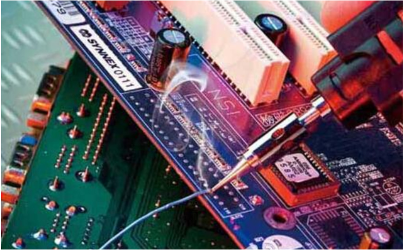
◆ Analysis of SMT reflow defects:
Solder Balls: Causes: 1. The silk screen hole is not aligned with the bonding pad, and the printing is inaccurate, which makes the solder paste dirty the PCB. 2. Solder paste is exposed too much in the oxidation environment and absorbs too much water in the air. 3. The heating is inaccurate, too slow and uneven. 4. The heating rate is too fast and the preheating interval is too long. 5. Solder paste dries too fast. 6. The activity of flux is not enough. 7. Too many small tin powders. 8. The volatility of flux is inappropriate during reflow. The process approval standard for solder balls is: when the distance between bonding pads or printed wires is 0.13mm, the diameter of solder beads cannot exceed 0.13mm, or no more than five solder beads can appear within 600mm square.
Bridging: Generally speaking, the reason for tin bridge is that the solder paste is too thin. SMT chip processing includes low metal or solid content in the solder paste, low shake solubility, easy squeezing of solder paste, too large solder paste particles, and too small surface tension of flux. There is too much solder paste on the bonding pad, and the peak value of reflow temperature is too high.
Open: Causes: 1. Insufficient solder paste. 2. The coplanarity of component pins is insufficient. 3. The tin is not wet enough (not melted enough, poor fluidity), and the solder paste is too thin, causing tin loss. 4. Solder absorption of pins (like rushes) or connecting holes nearby. Coplanarity of pins is particularly important for pin components with dense and ultra dense spacing. One solution is to tin the bonding pad in advance. Tin absorption of pins can be prevented by slowing down the heating speed and heating more at the bottom and less at the top. You can also use a flux with a slow wetting speed and high active temperature or a solder paste with different Sn/Pb ratios that retards melting to reduce the tin absorption of the pin.
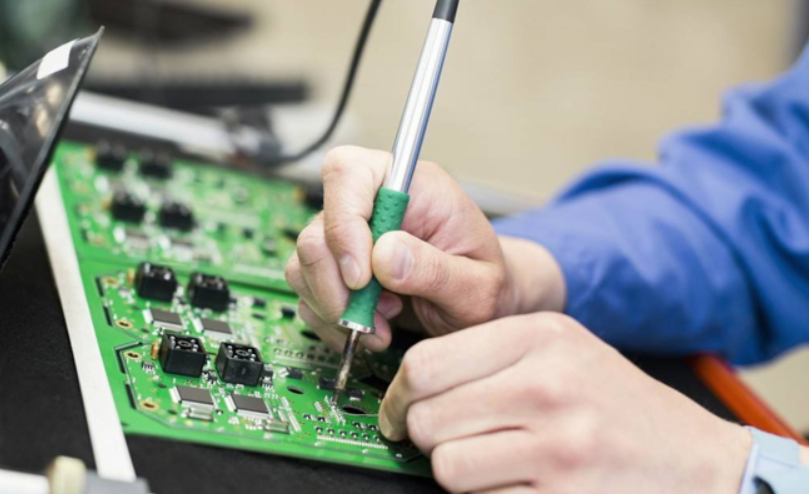
◆ Technical composition related to SMT
Design and manufacturing technology of electronic components and integrated circuits
Circuit Design Technology of Electronic Products
Manufacturing Technology of Circuit Board
Design and manufacturing technology of automatic mounting equipment
Circuit Assembly Manufacturing Process Technology
Development and production technology of auxiliary materials used in assembly and manufacturing
◆ Chip mounter:
Gantry:
The component feeder and the base plate (PCB) are fixed. The tip (with multiple vacuum suction nozzles installed) moves back and forth between the feeder and the base plate, takes the component out of the feeder, adjusts the component position and direction, and then pastes it on the base plate. The patch head is named because it is installed on the arch type X/Y coordinate moving beam.
Adjustment method for component position and direction: 1) Mechanical alignment adjustment position and suction nozzle rotation adjustment direction, which can achieve limited accuracy, are no longer used for later models. 2) Laser identification, X/Y coordinate system position adjustment, nozzle rotation direction adjustment. This method can realize identification during flight, but cannot be used for ball grid array element BGA. 3) Camera recognition, X/Y coordinate system adjustment position, suction nozzle rotation adjustment direction. Generally, the camera is fixed, and the tip flies over the camera for imaging recognition. It takes a little longer than laser recognition, but it can identify any element. There are also camera recognition systems that can realize recognition during flight. There are other sacrifices in mechanical structure.
The speed of this form is limited due to the long back and forth distance of the patch head. OEM OEM substitute materials now generally use multiple vacuum suction nozzles to take materials at the same time (up to ten) and double beam system to improve the speed, that is, when the tip on one beam is taking materials, the tip on the other beam is almost twice as fast as the single beam system. However, in practical application, it is difficult to achieve the conditions for simultaneous reclaiming, and different types of components need to be replaced with different vacuum suction nozzles, which will cause time delay.
The advantages of this type of machine are: simple system structure, high precision, suitable for various sizes and shapes of components, even special-shaped components. The feeder can be in the form of ribbon, tube or tray. It is suitable for medium and small batch production, and can also be combined with multiple machines for mass production.
Turret type:
The component feeder is placed on a single coordinate moving cart, the PCB base plate is placed on a moving workbench of the X/Y coordinate system, and the patch head is installed on a turret. When the cart is working, the component feeder is moved to the reclaiming position, the vacuum suction nozzle on the patch head is placed at the reclaiming position to take the components, and it is rotated to the placement position (180 degrees from the reclaiming position) through the turret. During the rotation, the component position and direction are adjusted, Place the component on the base plate.
Adjustment method for PCB component position and direction: 1) Mechanical alignment adjustment position, suction nozzle rotation adjustment direction, this method can achieve limited accuracy, and later models have no longer used. 2) Camera recognition, X/Y coordinate system adjustment position, suction nozzle self rotation adjustment direction, camera fixation, chip head flying over the camera for imaging recognition.
Generally, the turret is equipped with more than ten to twenty piece heads, and each piece head is equipped with 2-4 vacuum nozzles (earlier models) to 5-6 vacuum nozzles (current models). Due to the characteristics of the turret, the action is refined. The actions such as selecting and changing suction nozzles, moving the feeder in place, taking components, component identification, angle adjustment, worktable movement (including position adjustment), and placing components can be completed in the same time period, so the real high speed is achieved. At present, the fastest time period is 0.08~0.10 seconds for one element.
This model is superior in speed and suitable for mass production, but it can only use ribbon packed components. If it is a pin, large integrated circuit (IC), it can not be completed only by pallet packaging, so it also depends on the cooperation of other models. This kind of equipment is complex in structure and expensive in cost. The latest model is about US $500000, more than three times of the arch type.
PCBA factory inspection technology
Oct 25,2022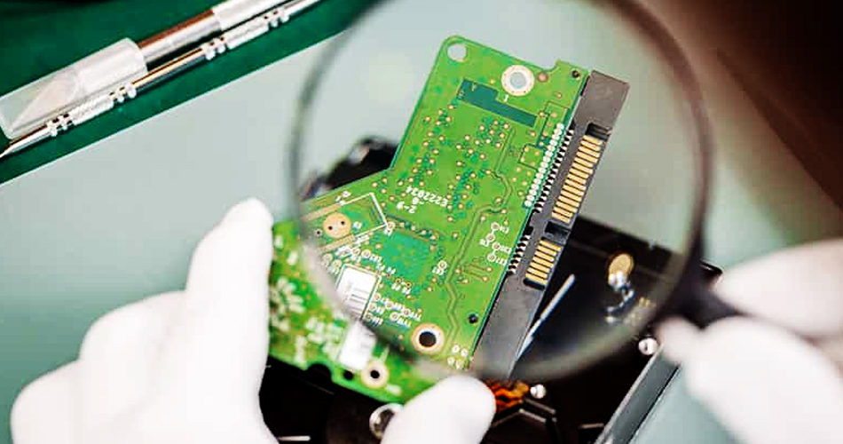


Just upload Gerber files, BOM files and design files, and the KINGFORD team will provide a complete quotation within 24h.