
Professional PCB manufacturing and assembly
Building 6, Zone 3, Yuekang Road,Bao'an District, Shenzhen, China
+86-13410863085Mon.-Sat.08:00-20:00

This article clarifies the concept of SMT, PCB, PCBA and DIP, and introduces in detail what SMT is, the difference between PCB and PCBA, what DIP is, and the difference between DIP and SOP.
1、 What does SMT mean? SMT is one of the basic components of electronic components. It is called surface mount technology (or surface mount technology). It is divided into no pin or short lead. It is a circuit assembly technology that is welded and assembled by reflow welding or dip welding, and is also the most popular technology and process in the electronic assembly industry.

Features: Our base plate can be used for power supply, signal transmission, heat dissipation and structure provision.
Characteristics: It can withstand the temperature and time of curing and welding.
The flatness shall meet the requirements of the manufacturing process.
Suitable for repair work.
Suitable for the manufacturing process of substrate.
Low dielectric number and high resistance.
The commonly used materials of our product baseplates are healthy and environment-friendly epoxy resin and phenolic resin, which have good flame resistance, temperature characteristics, mechanical and dielectric properties and low cost.
As mentioned above, the rigid substrate is solid.
Our products also have flexible substrates, which can save space, fold or turn, and move. They are made of very thin insulating sheets, and have good high-frequency performance.
The disadvantage is that the assembly process is difficult and is not suitable for micro spacing applications.
I think the characteristics of the substrate are small lead wires and spacing, large thickness and area, better thermal conductivity, harder mechanical properties, and better stability. I think the mounting technology on the substrate is electrical performance, reliability and standard parts.
We not only have a fully automatic and integrated operation, but also have the double guarantee of manual layer by layer audit, machine audit and manual audit. The product qualification rate is up to 99. 98%.
2、 PCB is one of the most important electronic components. Generally, printed circuit refers to the conductive pattern made of printed circuit, printed component or both on insulating material according to predetermined design. The conductive pattern on the insulating substrate that provides electrical connection between components is called printed circuit board (or printed circuit board). It is an important support of electronic components and can bear the carrier of components.
I think we can usually open the computer keyboard to see a soft film (flexible insulating substrate), printed with silver white (silver paste) conductive graphics and key graphics. Because this pattern is obtained by the general screen leakage printing method, we call this printed circuit board flexible silver paste printed circuit board. However, when we went to the computer city, we saw different kinds of printed circuit boards on computer mainboards, video cards, network cards, modems, sound cards and household appliances.
The base material used is made of paper base (commonly used for one side) or glass cloth base (commonly used for both sides and multiple layers), pre impregnated with phenolic or epoxy resin, one or both sides of the surface layer are pasted with copper coated sheet and then laminated for curing. This kind of circuit board copper clad thin plate is called rigid plate. The printed circuit board is then made, and we call it rigid printed circuit board.
The printed circuit board with printed circuit graphics on one side is called single-sided printed circuit board, and the printed circuit board with printed circuit graphics on both sides is called double-sided printed circuit board, which is formed by double-sided interconnection through the metallization of holes. If one double-sided printed circuit board is used as the inner layer, two single-sided printed circuit boards are used as the outer layer, or two double-sided printed circuit boards are used as the inner layer, and two single-sided printed circuit boards are used as the outer layer, the printed circuit boards that are alternately connected by the positioning system and the insulating bonding materials, and the conductive patterns are interconnected according to the design requirements, become four layer and six layer printed circuit boards, also known as multilayer printed circuit boards.
3、 PCBA is one of the basic components of electronic components. The whole process of surface mount technology (SMT) and DIP plug-in insertion of PCB is called PCBA process or PCBA processing. In fact, it is a PCB pasted with a piece. One is finished board and the other is bare board.
PCBA can be understood as a finished circuit board, that is, PCBA can only be counted after all processes of the circuit board have been completed. Due to the continuous miniaturization and refinement of electronic products, most of the current circuit boards are made of etched circuit boards after exposure and development by means of adhesive etching inhibitors (film pressing or coating).
In the past, the understanding of cleaning was not enough, because the assembly density of PCBA was not high. It was also believed that the residual flux was non-conductive and benign, and would not affect the electrical performance.
Today's electronic assemblies tend to be miniaturized, even smaller devices, or smaller spacing. The pins and bonding pads are getting closer and closer. Now the gap is smaller and smaller, and pollutants may also be stuck in the gap, which means that small particles, if left between the two gaps, may also cause the bad phenomenon of short circuit.
In recent years, the recognition and voice of the electronic assembly industry for cleaning are getting higher and higher, not only for products, but also for environmental requirements and protection of human health. Therefore, there are many suppliers of cleaning equipment and solutions, and cleaning has become one of the main contents of technical exchange and discussion in the electronic assembly industry.
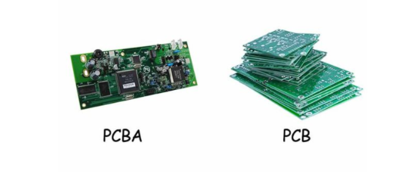
Differences between PCBA and PCB
PCB has many kinds of names, such as circuit board, circuit board, printed circuit board, etc. It is an important electronic component. As a bare board, PCB is used to mount electronic components, connect electronic components with circuit board, and achieve certain functions.
PCBA is the abbreviation of Printed Circuit Board Assembly. However, in foreign countries, PCBA is generally translated as PCB Assembly. PCBA is a finished product of PCB bare board after SMT mounting, DIP plug-in and PCBA testing, quality inspection and assembly. It can realize the design function of designers. Almost all electronic products, such as smart home, AR, VR, medical equipment, etc., need PCBA boards.
Differences between PCBA and PCB - Clarify the concept of SMT, PCB, PCBA and DIP
4、 DIP is one of the basic components of electronic components. It is called dual in line packaging technology. It refers to the integrated circuit chips packaged in dual in line format. It is also used in most small and medium-sized integrated circuits, and the number of pins generally does not exceed 100.
The CPU chip of DIP packaging technology has two rows of pins, which need to be inserted into the chip socket with DIP structure.
Of course, it can also be directly inserted into the circuit board with the same number of solder holes and geometric arrangement for soldering.
The DIP packaging technology shall be inserted and pulled out from the chip socket with special care to avoid damaging the pins.
Features: multi-layer ceramic dual in-line DIP, single-layer ceramic dual in-line DIP, lead frame DIP (including glass ceramic sealing type, plastic packaging structure type, ceramic low melting glass packaging type), etc.
DIP plug-in is a link in the electronic manufacturing process, including manual plug-in and AI plug-in. Insert the specified material into the specified position. Manual plug-ins also need wave soldering to weld electronic components on the board. For the inserted components, check whether they are inserted incorrectly or missed.
Post welding of DIP plug-in is a very important process in the processing of pcba chip, and its processing quality directly affects the function of pcba board. Its importance is very important. After welding, because some components cannot be welded by wave soldering machine according to the limitations of process and materials, they can only be welded manually.
This also reflects the importance of DIP plug-in in electronic components. Only by paying attention to details can we be perfect.
Differences between DIP and SOP
SOP packaging belongs to chip packaging. DIP (dual in line package). One of the plug-in packages, the pins are led out from both sides of the package, and the packaging materials are plastic and ceramic. DIP is the most popular plug-in package, and its application range includes standard logic IC, memory LSI, microcomputer circuit, etc. The pin center distance is 2.54mm, and the number of pins is from 6 to 64. The package width is usually 15.2mm. Some packages with a width of 7.52mm and 10.16mm are called skinny DIP and slim DIP respectively. However, in most cases, it is not differentiated and is simply referred to as DIP. In addition, ceramic DIPs sealed with low melting point glass are also called cerdip (see cerdip).
DIP is a direct plug-in chip, SOP is a chip chip, and the direct plug-in chip is directly inserted on the motherboard. SOP is not inserted, but is pasted on the motherboard. The number after DIP and sop represents the pin.
Difference between DIP and SOP - This article clarifies the concept of SMT, PCB, PCBA and DIP
In these four electronic components, each has its own advantages, but they complement each other to form this series of production process. Only by strictly controlling the quality of products produced by Wanlong Jingyi, can customers understand our intentions and ensure that the quality of products delivered from the warehouse reaches more than 96%.


Just upload Gerber files, BOM files and design files, and the KINGFORD team will provide a complete quotation within 24h.