
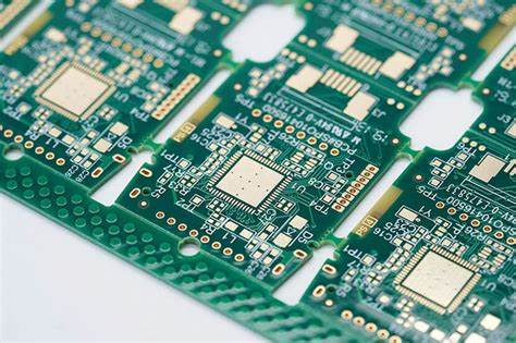
Professional PCB manufacturing and assembly
Building 6, Zone 3, Yuekang Road,Bao'an District, Shenzhen, China
+86-13410863085Mon.-Sat.08:00-20:00


Impedance design of PCB
1. Definition of impedance:
At a certain frequency, in the transmission signal line of an electronic device, relative to a certain reference layer, the resistance suffered by the high-frequency signal or electromagnetic wave during propagation is called characteristi
impedance.
During PCB production, it is determined whether impedance control is required according to customer requirements. If the customer requires impedance control for a certain line width, the impedance of this line width needs to becontrolled during production.
When the signal is transmitted on the PCB, the characteristic impedance of the PCB board must match the electronic impedance of the head and tail components. Once the impedance value exceeds the tolerance, the transmitted signal energy will appear reflection, scattering, attenuation or delay, etc., thus This leads to incomplete and distorted signals.
2. Tools for calculating impedance:
At present, most people use software: Si9000 and so on.
There are three main software impedance models commonly used: (1) characteristic impedance, also called single-ended impedance; (2) differential impedance, also called differential impedance; (3) coplanar impedance, also calledcoplanar waveguide impedance, mainly used in In the design of double-panel impedance.
The reason for choosing the coplanar impedance design is that the thickness of the double-sided board determines the distance of the impedance line. The reference plane below is relatively far away, and the signal is very weak. It is necessary to choose a reference plane with a closer distance, so the design of coplanar impedance is produced.
3. Open the Polar Si9000 software. Familiarize yourself with several commonly used impedance models:
(1) Theigure below f is the characteristic impedance model of the outer layer (also called the single-ended impedance model):
(2) The figure below is the differential impedance model of the outer layer:
(3) The inner differential impedance model is commonly used in the following three types:
The following are commonly used models for coplanarity:
(4) The following figure is the coplanar single-ended impedance model of the outer layer:
(5) The following figure is the coplanar differential impedance model of the outer layer:
4. How to calculate the impedance?
H1: Medium thickness (PP sheet or plate, not including copper thickness)
Er1: Dielectric constant of PP sheet (see specifications for each PP constant)
W1: line width on impedance line (line width required by customers)
W2: Impedance line width (W2=W1-0.5MIL)
S1: Impedance line spacing (customer original)
D1: Distance from impedance line to copper skin
T1: finished copper thickness
C1: The green oil thickness of the substrate (primary printing ink C1: 30UM/secondary printing ink C1: 60UM) 2OZ and above printed twice
C2: Thickness of green oil on the copper skin or wiring (primary ink C2: 12UM/secondary ink C2: 25UM) 2OZ and above printed twice
C3: The thickness of the green oil on the substrate (primary ink C3: 30UM/secondary ink C3: 60UM) 2OZ and above printed twice
Cer: Dielectric constant of green oil (according to 4.2MIL)
Zo: theoretical resistance calculated from the above parameters
Note:
A: The outer layer is copper foil thickness + copper plating thickness, which depends on the hole copper specification. When the bottom copper is HOZ, hole copper (average 20UM, minimum 18UM), surface copper is calculated as 45UM: hole copper (average 25UM, minimum 20UM), surface copper is calculated as 50UM: the minimum single point of hole copper is 25UM, and surface copper is calculated as 55UM.
B: When the base copper is 102, the hole copper (average 20UM, minimum 18UM), the surface copper is calculated as 55UM; the hole copper (average 25UM, minimum 20UM), the surface copper is calculated as 60UM; the hole copper single point minimum 25UM, Table copper is calculated according to 65UM.
The thickness and dielectric constant of various PP and their combinations are detailed in the PP specification table in the specification, and the copper thickness rules are in accordance with the completed copper thickness.
First calculate the outer impedance:
It can be seen that the single-ended line width of the outer layer is 4.5mil to meet 50 ohms.
In the above figure: H1 is the dielectric thickness of L1 to L2 layer (); Er1 is the dielectric constant of the medium; W2 is the upper line width; W1 is the lower line width; T1 refers to the thickness of the outer finished copper; C1, C2 are green oil Thickness; CEr refers to the dielectric constant of green oil; Z0 is the calculated impedance value; Calculate is the calculation button.
In the figure above: In the differential impedance calculation, S1 represents the differential line spacing;
(2) Let's talk about the calculation of inner layer impedance:The parameters are explained below:
Corresponding to the impedance of the L3 layer, the impedance line of the L3 layer is facing downward, so W2 is below; How to judge H1 and H2: The key is to find out the direction of the impedance line,
A PCB board has green oil, PP, and copper foil. PP can be superimposed on each other. Different PP corresponds to different dielectric constants, and of course the thickness is also different.
In the model, H1 is 4mil, H2=7.5+0.6=8.1mil, and 0.6mil is the copper thickness of L3 layer. The PP used in 7.5mil is: the combination of 1080+2116.
(3) Let's talk about a typical 8-layer board impedance:
NOTE: This data sheet will be used when calculating impedance below.
Note: When calculating the inner layer impedance, the difference between L3, L4 and L6 is used. Among them, the L6 layer impedance calculation model is the reference of the adjacent layer, which is the same as the above one.
When calculating the L3 and L4 layer impedance, the model used is: one of the interlayer references, the 1B2A model is used.
Now focus on how to calculate the impedance of L3 and L4 layers (the model used is shown in the figure below):
Parameter size setting, as shown in the figure above: H1=6.5mil; H2=22.44+0.6+0.6=23.64mil; H3=6.5mil;
In addition, the following items should be paid attention to when designing the impedance line:
(a) The distance between the differential lines should be as consistent as possible (parallel and equidistant);
(b) Attention: Integrity of impedance line shielding;
(C) When designing the impedance line width, the line width of the single-ended impedance line and the differential impedance should be distinguished, divided into three numbers, and different line widths are fine. For example: 5.1MIL, 4.9MIL, 5.0;
This is very important. Many customers design impedances on the same layer. Single-ended 50 ohms, differential 100 ohms, and 90 ohms use a line width of 5MIL, which is not advisable. The CAM engineer of the board factory finds the position of the impedance line by searching the D code of the line width in the CAM software. If they are all 5mil, it is difficult to distinguish, and it is very troublesome to provide a picture description.
FR4 Materials and Properties
Jun 04,2023


Just upload Gerber files, BOM files and design files, and the KINGFORD team will provide a complete quotation within 24h.