
Professional PCB manufacturing and assembly
Building 6, Zone 3, Yuekang Road,Bao'an District, Shenzhen, China
+86-13410863085Mon.-Sat.08:00-20:00

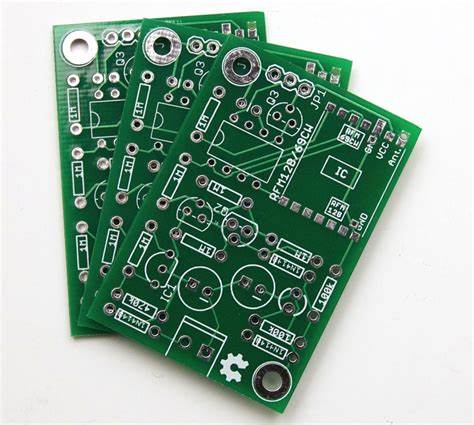
double PCB sided circuit board
Double-sided tin plate/immersion gold plate production process:
Cutting --- Drilling --- Immersion Copper --- Line --- Diagram --- Etching --- Soldering --- Characters --- HASL ( Or immersion gold)-gong edge-v cutting (some boards do not need)-----flying test--vacuum packaging
Double-sided gold-plated plate production process:
Cutting --- Drilling --- Immersion Copper --- Circuit --- Graphics --- Gold plating --- Etching --- Solder mask --- Characters -- ---Side edge---V cutting---Flying test---Vacuum packing
Multi-layer tin plate/immersion gold plate production process:
Cutting --- inner layer --- lamination --- drilling --- sinking copper --- wiring --- drawing --- etching --- solder mask ---Character--HASL (or immersion gold)-gong edge-v cutting (some boards do not need)-----flying test--vacuum packaging
The production process of multi-layer gold-plated board:
Cutting --- Inner layer ---Lamination ---Drilling --- Immersion Copper --- Circuit --- Graphics --- Gold Plating --- Etching -- --solder mask----characters-----gong edge---v cutting---flying test---vacuum packaging
1. Graphic electroplating process flow
Foil clad board --> blanking --> punching and drilling reference hole --> CNC drilling --> inspection --> deburring --> electroless thin copper plating --> electroplating thin copper --> inspection --> Brush board --> Film (or screen printing) --> Exposure and development (or curing) --> Inspection and repair board --> Pattern plating (Cn + Sn/Pb) --> Film removal --> Etching --> Inspection and repair board--> Nickel-plated gold-plated plug--> Hot melt cleaning--> Electrical continuity detection--> Cleaning treatment--> Screen printing solder mask pattern--> Curing--> Screen printing mark symbol--> Curing --> shape processing --> cleaning and drying --> inspection --> packaging --> finished product. In the process "electroless plating
The two processes of thin copper --> electroplating thin copper can be replaced by a process of "chemical thick copper plating", both of which have their own advantages and disadvantages. Graphical electroplating--etching double-faced metallized plates are typical in the 1960s and 1970s Process. In the mid-1980s, the solder mask over bare copper process (SMOBC) gradually developed, especially in the manufacture of precision double-sided panels, which has become the mainstream process.
2. SMOBC process
The main advantage of the SMOBC board is that it solves the solder bridging short circuit phenomenon between thin lines, and at the same time, because of the constant lead-tin ratio, it has better solderability and storage than hot-melt boards.
There are many ways to manufacture SMOBC boards. There are standard graphic electroplating subtraction method and then lead-tin SMOBC process; tin plating or immersion tin instead of electroplating lead-tin subtractive graphic electroplating SMOBC process; plugging or masking hole method SMOBC process ; Addition SMOBC process, etc. The following mainly introduces the SMOBC process of the pattern electroplating method and the SMOBC process of the lead-tin stripping method and the plugging method.
The pattern electroplating method and the SMOBC process of stripping lead and tin are similar to the pattern electroplating process. Changes occur only after etching.
Double-sided copper clad board --> According to the pattern electroplating process to the etching process --> Lead stripping --> Inspection --> Cleaning --> Solder mask pattern --> Nickel plating and gold plating of plugs --> Plug tape --> Hot air leveling --> Cleaning --> Screen printing marks --> Shape processing --> Cleaning and drying --> Finished product inspection --> Packaging --> Finished product.
3. The main process flow of plugging method is as follows:
Double-sided foil clad board --> Drilling --> Electroless copper plating --> Whole board electroplating copper --> Hole plugging --> Screen printing imaging (positive image) --> Etching --> Remove screen printing materials, Remove plugging material --> Cleaning --> Solder mask pattern --> Plug nickel plating, gold plating --> Plug tape --> Hot air leveling --> The following process is the same as above to the finished product.
The process steps of this process are relatively simple, and the key is to block the hole and clean the ink that blocks the hole.
In the hole plugging process, if the hole plugging ink and screen printing imaging are not used, but a special masking dry film is used to cover the holes, and then exposed to make a positive image, this is the masked hole process. Compared with the plugging method, it no longer has the problem of cleaning the ink in the hole, but it has higher requirements for masking the dry film.
The basis of the SMOBC process is to first make a metallized double-sided board with bare copper holes, and then apply the hot air leveling process
Mechanism of porosity edit broadcast
The drill bit first drills holes on the copper-clad board, and then undergoes electroless copper plating, and electroplates copper to form plated through holes. Both play a crucial role in hole metallization.
1. Mechanism of chemical copper precipitation:
In the manufacturing process of double-sided and multi-layer printed boards, it is necessary to metallize the non-conductive bare holes, that is, to implement electroless copper deposition to make them conductors. Electroless copper precipitation solution is a catalytic "oxidation/reduction" reaction system. Under the catalysis of Ag, Pb, Au, Cu and other metal particles, copper is deposited.
2. Copper plating mechanism:
The definition of electroplating is to use the power supply to push the positively charged metal ions in the solution to the conductor surface of the cathode to form a plating layer. Copper electroplating is an "oxidation/reduction" reaction. The copper metal anode in the solution oxidizes the copper metal on its surface to become copper ions. On the other hand, a reduction reaction occurs on the cathode, and copper ions are deposited as copper metal. Both of them are exchanged by liquid medicine, and the chemical action achieves the purpose of porosity, and the exchange effect directly affects the quality of porosity.
Miscellaneous plug hole edit broadcast
In the long-term production control process, we found that when the hole diameter reaches 0.15-0.3mm, the proportion of plug holes increases by 30%
1. The plug hole problem in the hole formation process:
When processing printed boards, most of the small holes of 0.15-0.3mm still use the mechanical drilling process. In the long-term inspection, we found that when the hole was drilled, impurities remained in the hole
The following are the main reasons for drilling plug holes:
When plugged holes appear in small holes, due to the small pore size, it is difficult to remove impurities in the small holes by high-pressure water washing and chemical cleaning before copper deposition, which prevents the exchange of liquid in the holes during the chemical copper deposition process and makes chemical copper deposition useless. .
When drilling, select the appropriate drill bit and backing plate according to the thickness of the stack, keep the substrate clean, do not reuse the backing plate, and the effective dust collection effect (using an independent dust collection control system) is a factor that must be considered to solve the plug hole.
The process and advantages of PCB assembly
May 30,2023


Just upload Gerber files, BOM files and design files, and the KINGFORD team will provide a complete quotation within 24h.