
Professional PCB manufacturing and assembly
Building 6, Zone 3, Yuekang Road,Bao'an District, Shenzhen, China
+86-13410863085Mon.-Sat.08:00-20:00

Multi-layer PCB stack structure
1.1 Selection and stacking principles of the number of layers
Determining the stacked structure of a multilayer PCB requires consideration of many factors. From the perspective of wiring, the more layers, the better the wiring, but the cost and difficulty of board making will also increase. For manufacturers, whether the stacked structure is symmetrical or not is the focus of PCB board manufacturing, so the selection of the number of layers needs to consider the needs of various aspects to achieve the best balance.
For experienced designers, after completing the pre-layout of components, they will focus on the analysis of the PCB wiring bottleneck. Combining with other EDA tools to analyze the wiring density of the circuit board; then integrate the number and types of signal lines with special wiring requirements such as differential lines, sensitive signal lines, etc. to determine the number of layers of the signal layer; then according to the type of power supply, isolation and anti-interference The requirements to determine the number of inner electrical layers. In this way, the number of layers of the entire circuit board is basically determined.
After determining the number of layers of the circuit board, the next job is to arrange the placement order of the circuits of each layer reasonably. In this step, the following two factors need to be considered.
(1) Distribution of special signal layers.
(2) Distribution of power supply layer and ground layer.
If there are more layers on the circuit board, there will be more types of arrangements and combinations of special signal layers, ground layers and power layers, and it will be more difficult to determine which combination is the best, but the general principles are as follows.
(1) The signal layer should be adjacent to an internal electrical layer (internal power supply/ground layer), and use the large copper film of the internal electrical layer to provide shielding for the signal layer.
(2) The internal power layer and the ground layer should be tightly coupled, that is to say, the dielectric thickness between the internal power layer and the ground layer should take a smaller value to increase the capacitance between the power layer and the ground layer and increase the resonance frequency . The dielectric thickness between the internal power layer and the formation layer can be set in Protel's Layer Stack Manager (layer stack manager). Select the [Design]/[Layer Stack Manager…] command, the system will pop up the layer stack manager dialog box, double-click the Prepreg text with the mouse, and the dialog box shown in Figure 11-1 will pop up, and you can change the insulation in the Thickness option of the dialog box layer thickness.
If the potential difference between the power supply and the ground wire is not large, a smaller insulation layer thickness can be used, such as 5mil (0.127mm).
(3) The high-speed signal transmission layer in the circuit should be a signal intermediate layer and sandwiched between two inner electrical layers. In this way, the copper films of the two inner electrical layers can provide electromagnetic shielding for high-speed signal transmission, and at the same time can effectively limit the radiation of high-speed signals between the two inner electrical layers, without causing external interference.
(4) Avoid direct adjoining of two signal layers. Crosstalk is easily introduced between adjacent signal layers, resulting in circuit function failure. Adding a ground plane between two signal layers can effectively avoid crosstalk.
(5) Multiple grounded internal electrical layers can effectively reduce grounding impedance. For example, the A signal layer and the B signal layer use separate ground planes, which can effectively reduce common-mode interference.
(6) Taking into account the symmetry of the layer structure.
1.2 Commonly used stacked structures
The following uses an example of a 4-layer board to illustrate how to optimize the arrangement and combination of various laminated structures.
For commonly used 4-layer boards, there are several stacking methods (from top layer to bottom layer).
(1) Siganl_1 (Top), GND (Inner_1), POWER (Inner_2), Siganl_2 (Bottom).
(2) Siganl_1 (Top), POWER (Inner_1), GND (Inner_2), Siganl_2 (Bottom).
(3) POWER (Top), Siganl_1 (Inner_1), GND (Inner_2), Siganl_2 (Bottom).
Obviously, scheme 3 lacks effective coupling between power plane and ground plane and should not be adopted.
So how to choose between Option 1 and Option 2? Under normal circumstances, designers will choose option 1 as the structure of the 4-layer board. The reason for the choice is not that option 2 cannot be used, but that the general PCB board only places components on the top layer, so it is more appropriate to use option 1. However, when components need to be placed on both the top layer and the bottom layer, and the dielectric thickness between the internal power layer and the ground layer is large, and the coupling is not good, it is necessary to consider which layer has fewer signal lines. For option 1, there are fewer signal lines on the bottom layer, and a large area of copper film can be used to couple with the POWER layer; on the contrary, if the components are mainly arranged on the bottom layer, then option 2 should be used to make the board.
If the stacked structure shown in Figure 11-1 is adopted, then the power layer and the ground layer are already coupled. Considering the requirement of symmetry, scheme 1 is generally adopted.
After completing the analysis of the stacked structure of the 4-layer board, an example of the combination of the 6-layer board is used to illustrate the arrangement and combination of the 6-layer board stacked structure and the optimal method.
(1) Siganl_1 (Top), GND (Inner_1), Siganl_2 (Inner_2), Siganl_3 (Inner_3), POWER (Inner_4), Siganl_4 (Bottom).
Solution 1 uses 4-layer signal layers and 2-layer internal power/ground layers, and has more signal layers, which is conducive to the wiring work between components. However, the defects of this solution are also obvious, which are manifested in the following two aspects.
① The power layer and the ground layer are far apart and not fully coupled.
② The signal layer Siganl_2 (Inner_2) and Siganl_3 (Inner_3) are directly adjacent to each other, the signal isolation is not good, and crosstalk is prone to occur.
(2) Siganl_1 (Top), Siganl_2 (Inner_1), POWER (Inner_2), GND (Inner_3), Siganl_3 (Inner_4), Siganl_4 (Bottom).
Compared with scheme 1, scheme 2 has sufficient coupling between the power layer and the ground layer, and has certain advantages over scheme 1, but the signal layers of Siganl_1 (Top) and Siganl_2 (Inner_1) and Siganl_3 (Inner_4) and Siganl_4 (Bottom) are directly Adjacent, the signal isolation is not good, and the problem of crosstalk prone to occur has not been solved.
(3) Siganl_1 (Top), GND (Inner_1), Siganl_2 (Inner_2), POWER (Inner_3), GND (Inner_4), Siganl_3 (Bottom).
Compared with Scheme 1 and Scheme 2, Scheme 3 reduces a signal layer and adds an internal electrical layer. Although the layers available for wiring are reduced, this scheme solves the common defects of Scheme 1 and Scheme 2.
① The power layer and the ground layer are tightly coupled.
② Each signal layer is directly adjacent to the internal electrical layer, effectively isolated from other signal layers, and crosstalk is not easy to occur.
③ Siganl_2 (Inner_2) is adjacent to two inner electrical layers GND (Inner_1) and POWER (Inner_3), which can be used to transmit high-speed signals. The two inner electrical layers can effectively shield the interference of the outside world on the Siganl_2 (Inner_2) layer and the interference of Siganl_2 (Inner_2) on the outside world.
Combining all aspects, Scheme 3 is obviously the most optimized one. At the same time, Scheme 3 is also a commonly used stacked structure for 6-layer boards.
2.1 General principles of component layout
The general principles that designers need to follow during the board layout process are as follows.
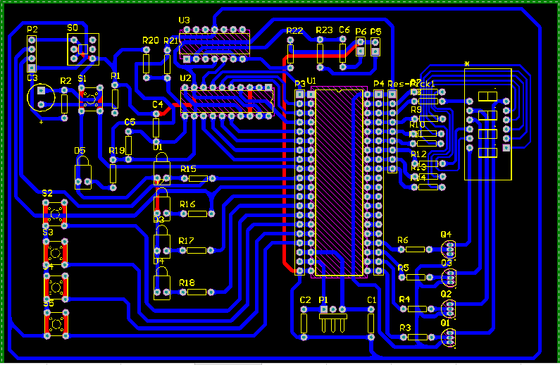
(1) Components are best placed on one side. If you need to place components on both sides, placing pin-type components on the bottom layer (Bottom Layer) may cause the circuit board to be difficult to place and not conducive to soldering, so it is best to only place SMD components on the bottom layer (Bottom Layer) , similar to the layout of components on the common computer graphics card PCB board. When placed on one side, only one side of the circuit board needs to be silk-screened, which is convenient for cost reduction.
(2) Reasonably arrange the position and direction of the interface components. Generally speaking, connector components used as a connection between the circuit board and the outside world (power supply, signal line), are usually arranged on the edge of the circuit board, such as serial ports and parallel ports. If it is placed in the center of the circuit board, it is obviously not conducive to wiring, and it may not be connected due to the obstruction of other components. In addition, when placing the interface, pay attention to the direction of the interface, so that the connecting wire can be drawn out smoothly and away from the circuit board. After the interface is placed, the type of the interface should be clearly marked with the String (character string) of the interface components; for the power interface, the voltage level should be marked to prevent the circuit board from being burned due to wiring errors.
(3) It is better to have a wide electrical isolation zone between high-voltage components and low-voltage components. That is to say, do not put components with very different voltage levels together, which is not only conducive to electrical insulation, but also has great benefits for signal isolation and anti-interference.
(4) Components with close electrical connections are best placed together. This is the idea of modular layout.
(5) For components that are prone to noise, such as high-frequency devices such as clock generators and crystal oscillators, they should be placed as close to the clock input end of the CPU as possible when placing them. High-current circuits and switching circuits are also prone to noise. When laying out these components or modules, they should also be kept away from high-speed signal circuits such as logic control circuits and storage circuits. If possible, try to use the control board combined with the power board. To connect to improve the anti-interference ability and work reliability of the circuit board as a whole.
(6) Try to place decoupling capacitors and filter capacitors around the power supply and chip. The arrangement of decoupling capacitors and filter capacitors is an important measure to improve the power quality of the circuit board and improve the anti-interference ability. In practical applications, the traces, pin connections, and wiring of the printed circuit board may bring large parasitic inductance, resulting in high-frequency ripples and burrs in the power supply waveform and signal waveform, while the power supply and ground A 0.1F decoupling capacitor placed between them can effectively filter out these high-frequency ripples and glitches. If chip capacitors are used on the circuit board, the chip capacitors should be placed close to the power pins of the components. For the power conversion chip or the power input terminal, it is best to arrange a 10F or larger capacitor to further improve the power quality.
(7) The numbers of components should be arranged close to the frame of the components, uniform in size, neat in direction, and not overlapping with components, vias and pads. The first pin of the component or connector indicates the direction; the positive and negative signs should be clearly marked on the PCB and are not allowed to be covered; power conversion components (such as DC/DC converters, linear conversion power supplies and switching power supplies) There should be enough space for heat dissipation and installation, and enough space for welding on the periphery.


Just upload Gerber files, BOM files and design files, and the KINGFORD team will provide a complete quotation within 24h.