
Professional PCB manufacturing and assembly
Building 6, Zone 3, Yuekang Road,Bao'an District, Shenzhen, China
+86-13410863085Mon.-Sat.08:00-20:00

How to judge the circuit design is good or bad there are the following points:
1. Standard rules for size and thickness. Customers can measure and check their own product thickness and specifications.
2. Light and color. External circuit boards are covered with ink, circuit boards can play the role of insulation, if the color of the board is not bright less ink, then PCB itself is not good.
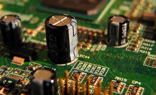
3. Appearance of weld. There are many PCB parts. If the welding is not good, the parts will fall off easily, which will seriously affect the welding quality.
4. After the installation of components, the telephone should be easy to use, that is, the electrical connection should meet the requirements.
5, line width, line thickness, line distance meet the requirements, so as to avoid line heating, open circuit, and short circuit.
6, by high temperature copper is not easy to fall off.
7, copper surface is not easy to oxidize, affect the installation speed, oxidation after use soon after bad.
8. No additional electromagnetic radiation.
9. The shape is not deformed, so as to avoid the deformation of the shell and dislocation of the screw hole after installation. Now the installation is mechanized, the hole position of the circuit board and the deformation error of the circuit and circuit design should be within the allowable range.
10. High temperature, high humidity and special environment should also be considered.
11. The mechanical properties of the surface should meet the installation requirements.
SCM development process
Direct loading of dry goods:
1. Identify customer needs
The primary task of SCM development is to analyze and understand the overall requirements of the project, and consider the use of the system environment, reliability requirements, maintainability and product costs and other factors
2. Analyze software and hardware functions
Because SCM development by software and hardware two parts. In the application system, some functions can be realized by hardware or software. The use of hardware can improve the real-time performance and reliability of the system. Using software to realize, can reduce the system cost, simplify the hardware structure. Therefore, in the overall consideration, we must comprehensively analyze the above factors, and reasonably formulate the proportion of hardware and software tasks.
3. Determine the single-chip microcomputer and required components required by customers
According to the needs of customers, we should choose the single chip microcomputer to meet the requirements of customers, in order to achieve the performance and stability of customer requirements.
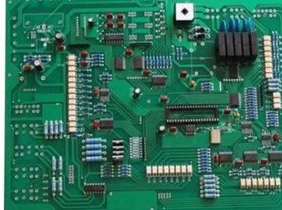
4. Circuit design
According to the design requirements and the selection of single chip microcomputer and components, we should design the corresponding circuit schematic
5. SCM software development
On the basis of system software design and circuit design, the program structure of the software system is determined and function modules are divided, and then the program design of each module is carried out.
6. Simulation and debugging
After the end of software development and circuit design, it is necessary to enter the integration and debugging phase of both. In order to avoid wasting resources, before generating the actual circuit board, you can use software for system simulation, problems can be modified in time. After the completion of the system simulation, using the drawing software, according to the circuit schematic PCB design, and then the PCB diagram to the relevant manufacturers to produce circuit boards. After getting the circuit board, in order to facilitate the replacement of devices and modify the circuit, you can first weld the required chip socket on the circuit board, and use the programmer to write the program into the single chip microcomputer. Next, plug the single chip microcomputer and other chips into the corresponding chip socket, connect the power supply and other input and output devices, and conduct system coordination until the debugging is successful.

7. Field test and user trial
Take the tested product to the scene used by the customer, conduct on-site debugging until the customer is satisfied, and then give the product to the customer for trial
8. End of the project
Understand PCB circuit board manufacturing process and method
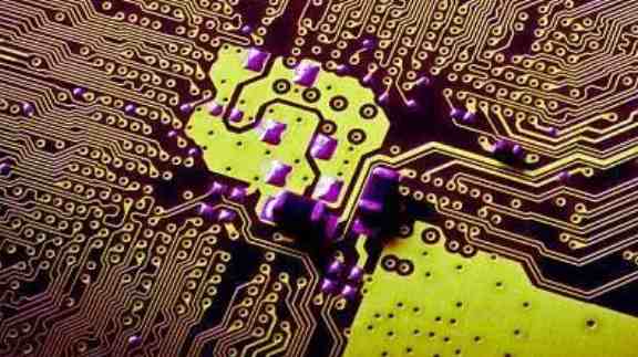
Printed circuit boards, also known as printed circuit boards, are providers of electrical connections to electronic components. It has a long history; Its design is mainly layout design; The main advantages of using circuit boards are greatly reduced wiring and assembly errors, and increased automation and productivity.
Composition of PCB
1. Dielectric layer: used to maintain the insulation between the circuit and the layer, commonly known as the substrate.
2 anti welding ink: not all the copper surface to eat tin part. Therefore, the non-tin-eating area will be printed with a layer of material (usually epoxy resin) to avoid short circuit between the non-tin-eating lines. According to the different technology, can be divided into green oil, red oil, blue oil.
3. Holes: conductive holes can make two or more stages of the circuit through each other, larger conductive holes can be used as parts plug-in. In addition, non-conductive holes are commonly used to position and secure screws during surface mounting during assembly.
4. Wiring and drawing: Wiring is used as a tool for the conduction between components. In the design, a large copper surface will be designed as the grounding and power layer. The line is concurrent with the drawing.
5. Screen printing: This is an unnecessary component, the main function is to mark the name and position of various parts on the circuit board, easy to maintain and identify after assembly.
6. Surface treatment: Because the copper surface is easy to oxidize in the general environment, it can not be tinned (poor solderability), so it will be protected in the copper surface that needs to eat tin. Protection methods include tin spraying (HASL), gold melting (ENIG), silver melting (silver leaching), tin melting (tin leaching) and organic flux retention (OSP). Each method has its own advantages and disadvantages, collectively known as surface treatment.


Just upload Gerber files, BOM files and design files, and the KINGFORD team will provide a complete quotation within 24h.