
Professional PCB manufacturing and assembly
Building 6, Zone 3, Yuekang Road,Bao'an District, Shenzhen, China
+86-13410863085Mon.-Sat.08:00-20:00

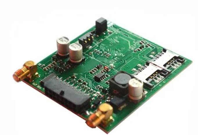
In order to improve the welding quality of PCBA processing of products, special processes need to be set up in each process. The manufacturing process of SMT patch processing is very complicated, and each process is linked with another one. Any problem in any process will affect the quality of products. In order to improve the welding quality of PCBA processing products, it is necessary to set up professional testing equipment in each process and strictly control the quality of the process. The following patch manufacturer would like to tell us what SMT patch processing and testing equipment and what relevant knowledge of SMT patch processing and diswelding skills are.
1. What are the SMT patch processing and dismantling skills
SMT chip processing parts to remove, generally speaking, it is not so easy. Practice regularly in order to master, otherwise, if forcibly removed, it is easy to destroy the SMD component. Of course, master... What are the disassembly and welding techniques for SMT patch processing? SMT chip processing parts to remove, generally speaking, it is not so easy. Practice regularly in order to master, otherwise, if forcibly removed, it is easy to destroy the SMD component. Of course, mastering these skills takes practice. SMT disassembly and welding processes are as follows:
1. For SMD components with fewer pins, such as resistors, capacitors, bipolar and triodes, tin plating is first done on a pad on the PCB board, then tweezers are used with the left hand to clamp the component to the mounting position and fix it to the circuit board, and the right hand to weld the pin on the pad to the sold pad. Iron. The left hand tweezers can be loosened and the rest of the foot can be welded with tin wire instead. This kind of element is also easy to disassemble, as long as both ends of the element and the soldering iron are heated at the same time, after melting the tin gently lift can be disassembled.
2. A similar method is used for patch components with more needles and wider spacing. First, the pad is tinned, then one foot is welded on the left side with a tweezer holding element, and the other foot is welded with a tin wire. It is usually better to remove these parts with a heat gun. On the one hand, a hand-held heat gun melts the solder, on the other hand, a clamp such as tweezers is used to remove the component while the solder melts.
3. For parts with high pin density, the welding process is similar, that is, one foot is welded first, and then the rest of the foot is welded with tin wire. The number of feet is large and dense, and the alignment of nails and pads is key. Typically, the corner pads are plated with very little tin and the parts are lined up with the pads with tweezers or by hand. Line up the edges of the pins.
These components are pressed slightly against the printed circuit board, and the corresponding pins on the pad are welded with soldering irons. The main recommended removal for high needle density parts is the heat gun, where the parts are held with tweezers, all pins are blown back and forth with the heat gun, and the parts are lifted when melted. If a part needs to be removed, it should not be blown to the center of the part for as short a time as possible. After removing the parts, clean the liner with a soldering iron.

2. What are the SMT patch processing and testing equipment
The manufacturing process of SMT patch processing is very complicated, and each process is one link after another. Any problem in any process will affect the quality of products. In order to improve the welding quality of PCBA processing of products, special processes need to be set up in each process. The manufacturing process of SMT patch processing is very complicated, and each process is linked with another one. Any problem in any process will affect the quality of products. In order to improve the welding quality of PCBA processing products, it is necessary to set up professional testing equipment in each process and strictly control the quality of the process. The following is the main introduction of SMT patch processing detection equipment are what?
SPI is the solder paste thickness measuring instrument, which is generally placed behind the solder paste printing process. It is mainly used to detect the thickness, area and volume distribution of the solder paste on the. I PCB boardt is an important equipment to monitor the solder paste printing quality.
2, AOI detection AOI is an automatic optical detector, which can be placed in various positions of the production line, but generally placed at the back of the reflow welding process, used to detect the welding quality of the PCB board after reflow welding, and timely find defects such as less tin, less material, virtual welding, tin and so on. Explain the importance of AOI testing equipment for SMT patch processing: During automatic detection, the machine automatically scans PCB through the camera, collects images, compares the solder joints tested with qualified parameters in the database, checks the defects on PCB through image processing, and displays/marks the defects through the display or automatic marks for SMT process engineers to improve and SMT maintenance personnel to repair. Automatic optical detector is widely used in SMT patch factories, which is gradually replacing manual detection.
3. X-RAY detection X-RAY is commonly used in hospitals. It uses high voltage impact on the target to generate X-ray penetration to detect the internal structural quality of electronic components, semiconductor packaging products, and SMT welding quality of various types of solder joints. It is mainly used to detect the BGA chip with the pin at the bottom, which can detect defects such as bridge, void, too large solder joint and too small solder joint on the BGA. Some objects that cannot be seen on the surface can be detected by X-RAY. The general price is relatively expensive, and the application is less in small and medium-sized enterprises.


Just upload Gerber files, BOM files and design files, and the KINGFORD team will provide a complete quotation within 24h.