
Professional PCB manufacturing and assembly
Building 6, Zone 3, Yuekang Road,Bao'an District, Shenzhen, China
+86-13410863085Mon.-Sat.08:00-20:00

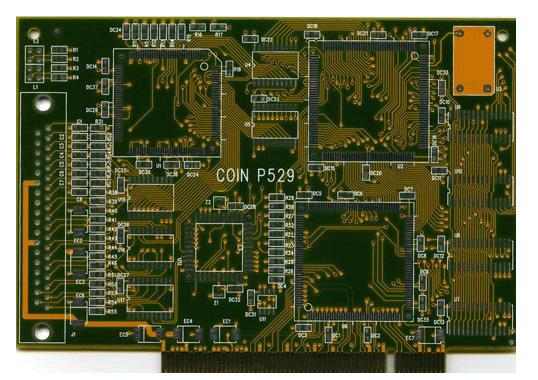
After the PCB design is completed, we need to check the function of all the items. Just as we finish the exam paper by ourselves, we should do a simple analysis and double check all the questions to make sure that we don't make big mistakes by negligence. Again, the PCB design is the same. The following patch processing manufacturer Xiaobian to explain how to evaluate the manufacturability of PCB design and how to eliminate PCBA processing short circuit fault related knowledge.
1. How to eliminate short circuit fault in PCBA processing?
kingford is a professional PCBA processing manufacturer providing overall PCBA electronic manufacturing services, including upstream electronic component procurement, PCB production and processing, SMT patch processing, DIP plug-in processing, PCBA testing, finished product assembly and other one-stop services. Here is how to eliminate PCBA processing short circuit fault.
Troubleshooting method of short circuit in PCBA processing
1. Open the PCB design drawing on the computer, light up the short-circuited network, and see where it is closest and most easily connected. Pay special attention to the IC internal short circuit.
Two, if it is artificial welding, to develop good habits:
1. Visually check the PCB board before welding, and use a multimeter to check whether the key circuit (especially the power supply and ground) is short circuit; 2. Every time after welding a chip, use a multimeter to test whether the power supply and ground short circuit; 3. Do not toss the soldering iron when welding. If the solder is thrown to the welding foot of the chip (especially the table sticker component), it is not easy to find.
3, there is a short circuit phenomenon. Take a board to cut the line (especially suitable for single/double layer board), after the cut line will each part of the functional block separately energized, step by step out. 4, the use of short-circuit positioning analysis instrument.
5, if there is a BGA chip, because all the solder joints are covered by the chip can not be seen, and it is a multilayer board (4 layers above), so it is best in the design of the power of each chip is divided, with a magnetic bead or 0 ohl resistance connection, so that when the power supply and ground short circuit, disconnect the magnetic bead detection, it is easy to locate to a chip. Because of the difficulty of BGA welding, if the machine is not automatic welding, a little attention will be the adjacent power and the ground two welding ball short circuit.
6, the small size of the sticker capacitor must be careful when welding, especially the power filter capacitor (103 or 104), the number is large, it is easy to cause short circuit between the power supply and the ground. Of course, sometimes, unfortunately, the capacitor itself will be short-circuited, so the best way is to check the capacitor before welding.

2. How do PCB designs evaluate manufacturability
1. DFM review of light plate: whether the production of light plate meets the technical requirements of PCB manufacturing, including line width, spacing, wiring, layout, through hole, marking, direction of wave soldering components, etc.
2. Check the consistency between the actual components and pad: whether the actual SMT patch components purchased are consistent with the design pad (if not, please indicate with a red label), and whether they meet the spacing requirements of the SMT patch machine.
3. Generate 3D graphics: Generate 3D graphics to check whether space elements interfere with each other, whether the layout of elements is reasonable, whether it is conducive to heat dissipation, and whether it is conducive to SMT reflow welding heat absorption.
4. Optimization of PCBA production line: optimization of charging sequence and location of material station. Input the existing pasting machine (such as Siemens high-speed machine, universal multifunctional machine) into the software, the components to be pasted are allocated to the existing board, how many kinds of pasting Siemens, how many kinds of pasting Siemens, how many kinds of pasting methods, how many kinds of pasting methods in the world, how many locations and in which station to take materials, etc. This can optimize SMT chip processing procedures, save time. For multiline production, the allocation of installation components can also be optimized.
5. Operation instructions: automatically generate the operation instructions of the workers on the production line.
6. Revision of inspection rules: Inspection rules can be modified. For example, the component spacing is 0.1mm, which can be set to 0.2mm depending on the specific model, manufacturer, and board complexity: the line width is 6mi, which can be changed to 5mil in high-density designs.
7. Support Panasonic, Fujifilm, global patch software: can automatically generate paste software, save programming time.
8. Automatically generate steel plate optimization graphics.
9. Automatic generation of AOI, X-ray program.
10. Check support for multiple software formats (Japanese, American KATENCE, Chinese PROTEL).
11. Check BOM and correct relevant errors, such as manufacturer's spelling mistakes. The BOM is converted to the software format. PCB design capability maximum signal design rate: 10Gbps CML differential signal; Maximum number of PCB design layers: 40; Minimum line width: 2.4mil; Minimum line spacing: 2.4mil; Minimum BGA PIN spacing: 0.4mm; Minimum mechanical hole diameter: 6mil; Minimum laser drilling diameter: 4mil; Maximum number of pins:; 63000+ Max number of components: 3600; Maximum number of BGA: 48+.
PCB design service process
1. The customer provides schematic diagram to consult PCB design; 2. Evaluate quotation according to schematic diagram and customer design requirements; 3. The customer confirms the quotation, signs the contract and pays the project deposit; 4. Received advance payment and arranged engineer design; 5. After the design is completed, provide the screenshot of the document to the customer for confirmation; 6. The customer confirmed OK, settled the balance, and provided PCB design materials.
How to deal with PCBA processing correctly
Feb 04,2023


Just upload Gerber files, BOM files and design files, and the KINGFORD team will provide a complete quotation within 24h.