
Professional PCB manufacturing and assembly
Building 6, Zone 3, Yuekang Road,Bao'an District, Shenzhen, China
+86-13410863085Mon.-Sat.08:00-20:00

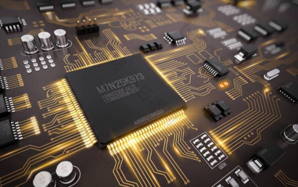
PCBA processing power graphic design considerations
As the main force of electronic industry, PCBA processing plant plays an important role in the development of electronic industry Professional PCBA processing plants are constantly updated and repeatedly calculated The following describes the precautions for power plane design in the patch
The processing of PCBA processing power board plays a key role in its design. In the detailed PCB design, the power solution can determine that 30% of the new projects are less than or equal to 50% of the qualified rate, so what should be paid attention to in the plane processing of the power supply?
1. In order to solve the problem of switching power supply, its current carrying capacity should be considered first, which includes two levels.
2. Whether the size and number of holes in the switch layer consider the working capacity of the commercial current of the switching power supply. First of all, we must master the bearing capacity of single hole. Under basic conditions, the temperature is 10 degrees.
A 10ml through-hole can withstand 1A current. This, if the switching power supply is 2A current when making the PCBA design scheme, at least 2 holes shall be made when using the 10 mil opening and replacement layer. Generally speaking, when designing a printed circuit board, you will consider the safe channel of the switching power supply to make more holes to keep a small margin.
2. The relative path of switching power supply shall be considered, and the following two levels shall be considered in practice.
1. The relative path of switching power supply shall be as short as possible. If the time is too long, the voltage drop of switching power supply will be serious, which will lead to the failure of new projects.
2. Try to keep the plane cutting of the power supply, and do not cut long rods and barbells.
3. When the switching power supply is divided, the separation distance between the switching power supply and the power plane should be kept at 20ml as far as possible. If in some BGA, 10ml spacing can be partially maintained, if the power plane is too close to the plan, there is a risk of short circuit fault.
4. If switching power supply is solved in adjacent solutions, copper coating or parallel surface wiring must be minimized. The key is to reduce the dry deflection between different switching power supplies, especially in some switching power supplies with large working voltage distance. Power planes must be prevented from overlapping. If unavoidable, the geological structure of medium distance can be considered.
3. When disconnecting the switching power supply, minimize the crossing of adjacent power lines. When the data signal is cut off (bright red power line has cross condition), the lack of continuous characteristic impedance in the reference scheme will lead to sudden change of characteristic impedance, which will lead to electromagnetic interference and crosstalk problems. In high-speed design schemes, cross branching does great harm to the quality of data signals.
Therefore, this PCBA power supply graphic design is a very important link, which is also a successful approval for PCBA to process plants


Just upload Gerber files, BOM files and design files, and the KINGFORD team will provide a complete quotation within 24h.