
Professional PCB manufacturing and assembly
Building 6, Zone 3, Yuekang Road,Bao'an District, Shenzhen, China
+86-13410863085Mon.-Sat.08:00-20:00

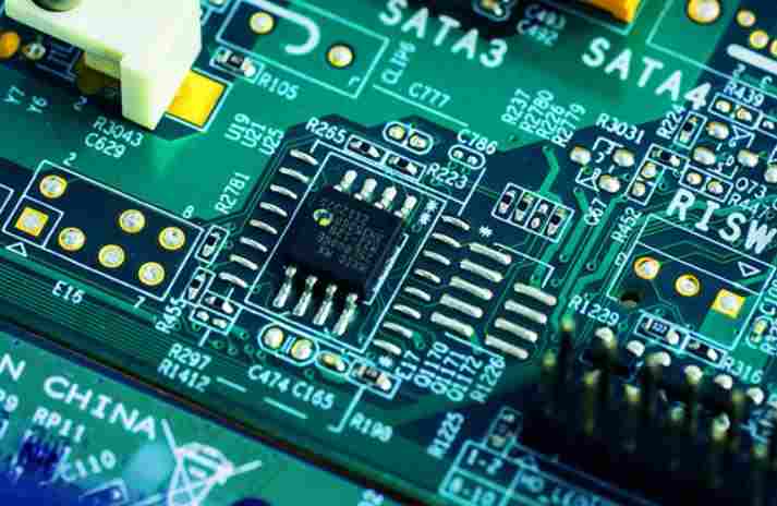
SMT inspection of incoming materials and mounters
The previous check SMT chip processing is the first condition to ensure the chip quality The quality of electronic components, printed circuit board, and smt chip data directly affect the quality of PCB Therefore, the power performance parameters of electronic components, the solderability of solder tips and solder legs, the productivity design of printed circuit boards, the solderability of solder pads, the quality agency of solder paste, repair glue, bar solder, flux, cleaning patch and other patch materials must have strict incoming inspection and management systems It is difficult or even impossible to solve the quality problems of electronic components, printed circuit boards and smt mounting materials in the subsequent process
Inspection of smt chip electronic components:
The main inspection items of electronic components include solderability, pin coplanarity and usability, which shall be sampled by the inspection department. To test the solderability of electronic components, stainless steel tweezers can clamp the main body of electronic components, immerse it in a tin pot at 235 ± 5 ℃ or 230 ± 5 ℃, and take it out at 2 ± 0.2s or 3 ± 0.5s. Check the welding end of the solder under a 20x microscope. The welding amount of the electronic component welding end is required to exceed 90%.
1. Visually inspect or use a magnifying glass to check whether the welding end or pin surface of electronic components is oxidized or free of contaminants.
2. The nominal value, specification, model, accuracy and overall dimensions of electronic components shall meet the product process requirements.
3. The SOT and SOIC pins are not deformed. For multi wire QFP devices with wire spacing less than 0.65mm, the coplanarity of the pins should be less than 0.1mm (optical detection can be performed through the mounter).
4. For products to be cleaned, the marks of electronic components will not fall off after cleaning, and will not affect the efficiency and reliability of electronic components (visual inspection after cleaning).
What is the method for SMT to place the machine with double-sided circuit boards installed?
With the increasing versatility and integration of current circuit boards, double-sided mounting circuit boards have been widely used, and the final products are becoming smaller and more intelligent. The small PCB circuit board is full of electronic components with various functions. It is necessary to make full use of the A side and B side of the circuit board.
After the components are installed on the A side of the circuit board, the components on the B side need to be printed again. At this time, side A and side B will reverse. The upper one will now flip to the bottom, and the lower one will flip to the top. This is only the first step. What is more troublesome is that SMT reflow soldering must be carried out again, because some components, especially BGA, are very strict with the welding temperature. If the solder paste is heated and melted during the second reflow soldering, and there are heavy parts on the bottom surface (first side), the equipment may fall or move due to its own weight and the melting and loosening of the solder paste. The quality is abnormal. In the process control of PCBA processing, when welding heavy components, we will choose reflow welding during the second welding.
What is the method for SMT mounter to install double-sided circuit board?
In addition, when there are many BGA and IC components on the circuit board, because some falling off and solder reflow problems must be eliminated, important components will be placed on the second side to make parts. In summary, it can only be completed by one reflow furnace good For other parts with fine pins, the alignment accuracy is required. If DFM allows, whether the equipment can be installed on the first side is more effective than that on the second side Better accuracy control Because when PCB is in the first reflow furnace, under the influence of high temperature welding, it will bend and deform invisible to the naked eye, but it will affect the welding of some tiny pins At the same time, the problem is that it will cause slight offset in solder paste printing, and the amount of the second solder paste is difficult to control
The above is the method for SMT mounter to install double-sided circuit board. Of course, due to the influence of the manufacturing process, some parts do not participate in the selection of side A and side B. The welding quality can be optimized by selecting the welding with the least influence on the process.
Reasons for SMT red glue drawing process
Dec 28,2022


Just upload Gerber files, BOM files and design files, and the KINGFORD team will provide a complete quotation within 24h.