
Professional PCB manufacturing and assembly
Building 6, Zone 3, Yuekang Road,Bao'an District, Shenzhen, China
+86-13410863085Mon.-Sat.08:00-20:00

Surface mount for mixed assembly of lead and lead-free BGA
1 Introduction
This SMT lead-free process has been widely used. However, the lead process is still used in military electronics manufacturing, but these components cannot be purchased with lead Lead and lead-free co-exist At present, I have all clues/lead-free BGA devices are usually used for joint assembly, because the melting point of lead-free solder ball is different from that of lead-free solder ball. For example, the melting point of lead-free BGA using Sn Ag Cu alloy is 2.17 ℃ higher than that of alloy lead BGA when Sn63-37Pb is used If the temperature curve of Sn63-37Pb solder is used, the peak temperature is usually 210230 ℃ Assuming that the peak temperature of PBGA is 220 ℃, when the temperature rises to 183 ℃, Sn-37Pb solder paste printed on the pad begins to melt At this time, the Sn Ag Cu solder ball of lead-free PBGA is not melted; When the temperature rises to 220 ℃, after welding, the temperature will begin to drop according to the lead process, and the lead-free solder ball has just melted Although the nominal melting point of Sn Ag Cu alloy is 217 ℃, in fact, Sn Ag Cu alloy is not a real eutectic alloy The liquidus temperature range is 216 è ½ 220℃. Therefore, the temperature at the end of lead process cooling and solidification is just the temperature when lead-free Sn Ag Cu solder ball just melted. It is in a paste state, where solid and liquid phases coexist When the solder ball melts, the solder ball begins to sink due to the gravity of the equipment During equipment sinking, PCB has slight vibration or deformation, which will damage the original welding interface structure on the side of PBGA assembly and cannot form new interface metal The alloy interlayer may lead to the failure of PBGA and solder joint side From the above, it can be seen that the temperature characteristics of the two solders/lead-free mixed assembly process should be considered in lead, and smaller process windows are more difficult
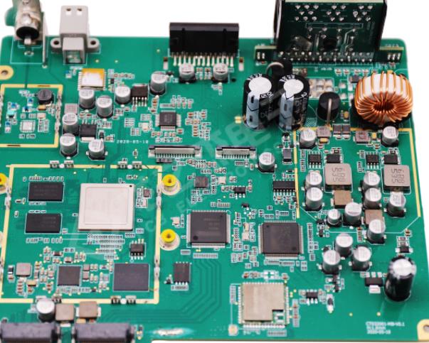
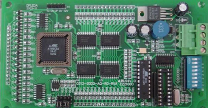
Pcba board

In order to obtain reliable welding products in mixed assembly, we should not only pay attention to the assembly and welding links, but also start from the first, middle and last three links of assembly, strengthen the whole process control, treat them differently according to the specific situation, and adjust the assembly production plan in time to make it more targeted, so as to obtain reliable products. Taking the process test as an example, the following lists the key points for strengthening the control of each link.
2 Process test
2.1 Test introduction
There are two cases of lead/lead-free BGA mixed assembly. One is that the number of lead-free devices accounts for the majority, or there are lead-free BGA devices with large size, and the compatible welding process curve is used for welding. This is the lead-free process curve. On this basis, the temperature shall be reasonably increased to control the peak temperature within the range of 230-235 ℃, so that the lead-free BGA device will not be damaged while meeting the reflow temperature required by the lead-free BGA device, so as to achieve better welding; The second is the number of lead devices in most cases. The size of lead-free BGA devices is small. The lead-free devices can be converted to lead devices through the ball planting process, and then the lead process curve can be used for welding.
In this experiment, two test boards are used: PCB 2 and polychlorinated biphenyl 4. The size of the test board is 100 * 150 mm. The device uses Sn63-37Pb tin lead and Sn Ag Cu solder ball data lead-free PBGA virtual sheet. The PCB thickness is 1.6 mm
2.1.1 Selection of test board
2.1.2 Equipment
PCB2: D2, D3 and D5 are lead-free false pieces, D1 and D6 are lead-free false pieces for welding after ball planting.
PCB4: D2, D3 and D7 are lead-free analog boards, and D1, D5, D6 and D8 are lead-free analog boards.
2.2 Preparation before assembly
Check the printed board and BGA device itself before assembly. The specific inspection contents are as follows.
(1) Printed board: no obvious warpage; There shall be no short circuit or open circuit on the base plate; The pad shall be free of characters, solder mask and other contamination; Printed circuit boards with serious oxidation, poor processing quality, serious surface pollution and other quality problems cannot be assembled and treated as unqualified products (as shown in Figure 2); For PCB with dirty surface, after cleaning for 2-3 times, squeeze and dry it with absorbent cotton ball dipped in absolute ethanol before welding to ensure that the surface of PCB is clean. Clean it before welding.
(2) BGA element: distinguish the BGA element to be assembled from the lead-free/lead-free element, and check whether the BGA solder ball has oxidation and defects.
2.3 Assembly
(1) In order to eliminate the adverse effects of moisture evaporation in high temperature welding, it is necessary to pre bake BGA devices and circuit boards. The specific method is: place the BGA device in an oven at 120 ℃ for 48 hours; Printed board 110 ℃, 4 hours.
(2) When printing solder paste, the solder paste shall cover more than 75% of the area of the bonding pad, and the surface of the solder paste shall be smooth, uniform, free of gaps, and shall not be short circuited to adjacent bonding pads, nor adhered to the substrate around the bonding pad. The waiting time between solder paste printing and reflow soldering shall be controlled within 2 hours.
(3) Set welding curve
It should be noted that the welding process curve parameters listed below were obtained during the PCB test used in this test. In production, the welding curve shall be adjusted and set according to the actual situation of the plate, such as the size, number of layers, equipment type, number of elements, distribution, etc.
the number of lead-free BGA devices on the board is larger than the number of lead devices. In this regard, consider setting the compatibility curve of welding and determining the parameters after multiple tests and adjustment of the curve


Just upload Gerber files, BOM files and design files, and the KINGFORD team will provide a complete quotation within 24h.