
Professional PCB manufacturing and assembly
Building 6, Zone 3, Yuekang Road,Bao'an District, Shenzhen, China
+86-13410863085Mon.-Sat.08:00-20:00

Surface Mount Technology Surface Wettability and Processing Characteristics
Surface wettability SMT patch treatment
Surface wetting in SMT wafer processing refers to the phenomenon that the solder diffuses and covers the metal surface to be welded during welding. SMT wafer surface wetting usually occurs when the liquid solder is in close contact with the metal surface to be welded. Only close contact can have sufficient attraction. Accordingly, when there are contaminants on the surface of the weld metal, close contact is not allowed. In the absence of pollutants, when solid substances and liquid substances come into contact during SMT patch processing, once an interface is formed, degradation will occur. The adsorption of surface energy, liquid substances will diffuse to the surface of solid substances, which is called wetting phenomenon.
In the immersion test, the patterned surface taken out of the molten solder bath will have the following phenomena:
1. Non wetting
The surface is restored to the state before it is uncovered, and the original color of the welding surface remains unchanged.
2 Wetting
3. Partially wetted
Some areas of the welding surface appear to be wet and some areas are not.
4 Weak wetting:
The surface of the metal to be welded is initially wetted, but after a period of time, the solder will shrink from a part of the welding surface to a liquid drop, and finally only a thin layer of solder will be left in the weakly wetted area.
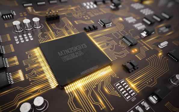
SMT wafer processing is also surface mount technology The specific content refers to placing wafer like components or small components suitable for surface assembly on the surface of PCB as required, and then welding with reflow soldering and other welding processes, Complete the assembly technology of electronic components The SMT circuit board, solder joints and components are located on the same side of the circuit board, The diameter of the hole is also much smaller This design can greatly improve the installation density of PCB components
1. Miniaturization
The size and volume of wafer components used in SMT wafer processing are much smaller than those of traditional wafers, which can generally be reduced by 60% - 70%, or even 90% The weight is reduced by 60% to 90% This can meet the development needs of miniaturization of electronic products
2. High signal transmission rate
The PCB board processed by SMT chip has compact structure and high placement density, which can achieve the effect of short connection and low delay, thus realizing high-speed signal transmission. At the same time, electronic products can be more resistant to vibration and shock.
3. High frequency characteristic
SMT chip processing components are usually lead-free or short leads, which reduces the distribution parameters of the circuit, thereby reducing RF interference.
4. It is beneficial to automatic production
SMT wafer processing components have many characteristics, such as size standardization, serialization and uniform welding conditions, which can make SMT wafer processing highly automatic.
5. Low data cost
The packaging cost of most PCBA chip processing components has been lower than that of the same type and function of chip processing components.
6. High production efficiency
SMT placement technology simplifies the production process of electronic products and reduces production costs. The whole production process is shortened and the production efficiency is improved
Surface wettability SMT patch treatment
Surface wetting in SMT wafer processing refers to the phenomenon that the solder diffuses and covers the metal surface to be welded during welding. SMT wafer surface wetting usually occurs when the liquid solder is in close contact with the metal surface to be welded. Only close contact can have sufficient attraction. Accordingly, when there are contaminants on the surface of the weld metal, close contact is not allowed. In the absence of pollutants, when solid substances and liquid substances come into contact during SMT patch processing, once an interface is formed, degradation will occur. The adsorption of surface energy, liquid substances will diffuse to the surface of solid substances, which is called wetting phenomenon.
In the immersion test, the patterned surface taken out of the molten solder bath will have the following phenomena:
1. Non wetting
The surface is restored to the state before it is uncovered, and the original color of the welding surface remains unchanged.
2 Wetting
3. Partially wetted
Some areas of the welding surface appear to be wet and some areas are not.
4 Weak wetting:
The surface of the metal to be welded is initially wetted, but after a period of time, the solder will shrink from a part of the welding surface to a liquid drop, and finally only a thin layer of solder will be left in the weakly wetted area.
SMT wafer processing is also surface mount technology The specific content refers to placing wafer like components or small components suitable for surface assembly on the surface of PCB as required, and then welding with reflow soldering and other welding processes, Complete the assembly technology of electronic components The SMT circuit board, solder joints and components are located on the same side of the circuit board, The diameter of the hole is also much smaller This design can greatly improve the installation density of PCB components
1. Miniaturization
The size and volume of wafer components used in SMT wafer processing are much smaller than those of traditional wafers, which can generally be reduced by 60% - 70%, or even 90% The weight is reduced by 60% to 90% This can meet the development needs of miniaturization of electronic products
2. High signal transmission rate
The PCB board processed by SMT chip has compact structure and high placement density, which can achieve the effect of short connection and low delay, thus realizing high-speed signal transmission. At the same time, electronic products can be more resistant to vibration and shock.
3. High frequency characteristic
SMT chip processing components are usually lead-free or short leads, which reduces the distribution parameters of the circuit, thereby reducing RF interference.
4. It is beneficial to automatic production
SMT wafer processing components have many characteristics, such as size standardization, serialization and uniform welding conditions, which can make SMT wafer processing highly automatic.
5. Low data cost
The packaging cost of most PCBA chip processing components has been lower than that of the same type and function of chip processing components.
6. High production efficiency
SMT placement technology simplifies the production process of electronic products and reduces production costs. The whole production process is shortened and the production efficiency is improved


Just upload Gerber files, BOM files and design files, and the KINGFORD team will provide a complete quotation within 24h.