
Professional PCB manufacturing and assembly
Building 6, Zone 3, Yuekang Road,Bao'an District, Shenzhen, China
+86-13410863085Mon.-Sat.08:00-20:00

Application of Internet+in SMT chip processing industry
In order to better apply "Internet+" to the processing and manufacturing of SMT electronic products, pay attention to the integration and aggregation of offline resources, the construction and promotion of network platforms, and actively explore new e-commerce marketing models
Gather senior management and technology teams in the industry, rely on the one-stop Internet service platform realized by "f2cpcb cloud manufacturing" electronic products, and integrate resources such as product design companies, supply chains, and manufacturing plants to provide customers with electronic product design, material procurement, and one-stop manufacturing services. Provide cost-effective services for enterprises, produce high-quality products for enterprises, and help enterprises improve their core competitiveness.
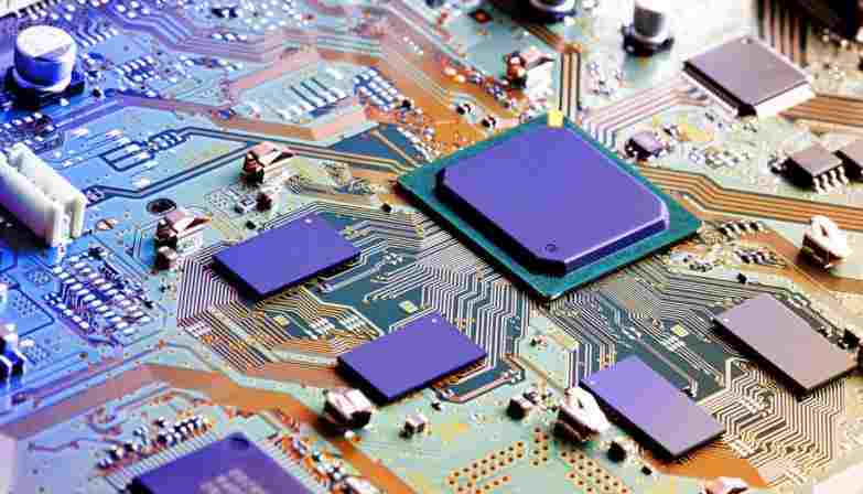
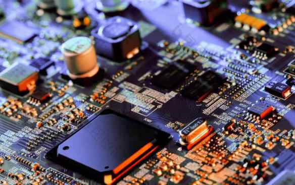
SMT processing chip technology greatly improves the efficiency of electronic assembly Surface mount technology includes: printing solder paste on PCB, installing components, reflow soldering, etc The key equipment of SMT processing is SMT machine The placement accuracy, placement speed and the application range of the placement machine determine the technical performance of the placement machine, and the placement machine also determines the efficiency of the SMT production line The manufacturing of electronic products can be divided into three levels
The top level is the manufacturing of complete products directly facing the end users, such as computer manufacturing, communication equipment, and various audio and video products The intermediate layer is a variety of electronic basic products that form electronic terminal products, including semiconductor integrated circuits, electronic vacuum and photoelectric display devices, electronic components, and electromechanical components Electronic products are assembled from basic electronic products The lowest level is special equipment, electronic measuring instruments and electronic special data that support the assembly of electronic terminal products and the production of electronic basic products They are the foundation and support of the entire electronic information industry
The composition and manufacturing process of electronic products can be summarized as the following technologies.
1. Micromachining technology.
Micro nano machining, micro machining and some precision machining technologies used in electronic manufacturing are collectively referred to as micro machining. Micro nano machining is basically a planar integration method in micro machining technology. The basic idea of planar integration is to build micro/nano structures by stacking planar substrate data layer by layer. In addition, cutting, welding, 3D printing, etching, sputtering and other processing methods using photon beam, electron beam and ion beam also belong to micro processing.
2. Interconnection packaging technology.
Interconnection between the wafer and the outgoing circuit on the substrate, such as flip chip welding, wire bonding, silicon through hole (TSV) and other technologies, as well as packaging technology after the wafer and the substrate are interconnected. These technologies are often referred to as chip packaging technologies. Passive component manufacturing technology. Including the manufacturing technology of passive components, such as capacitors, resistors, inductors, transformers, filters and antennas.
3. Photoelectric packaging technology.
Optoelectronic packaging is the systematic integration of optoelectronic devices, electronic components and functional application data. In the optical communication system, optoelectronic packaging can be divided into chip integrated circuit level packaging, device packaging and die MEMS manufacturing technology. A micro system that integrates sensors, actuators, and processing control circuits on a single silicon chip using micro fabrication techniques.
4. SMT electronic assembly technology
Electronic assembly technology is often called board level packaging technology. Electronic assembly technology is mainly based on surface assembly and through hole insertion technology. Electronic material technology. Electronic materials refer to materials used in electronic technology and microelectronic technology, including dielectric materials, semiconductor materials, piezoelectric and ferroelectric materials, conductive metals and their alloys, magnetic materials, optoelectronic materials, electromagnetic wave mask materials and other relevant materials. The preparation and application of electronic materials are the basis of electronic manufacturing technology.
The above is the explanation given by the editor of pcb circuit board company.
If you want to know more about PCBA, you can go to our company's home page to learn about it.
In addition, our company also sells various circuit boards,
High frequency circuit board and SMT chip are waiting for your presence again.


Just upload Gerber files, BOM files and design files, and the KINGFORD team will provide a complete quotation within 24h.