
Professional PCB manufacturing and assembly
Building 6, Zone 3, Yuekang Road,Bao'an District, Shenzhen, China
+86-13410863085Mon.-Sat.08:00-20:00

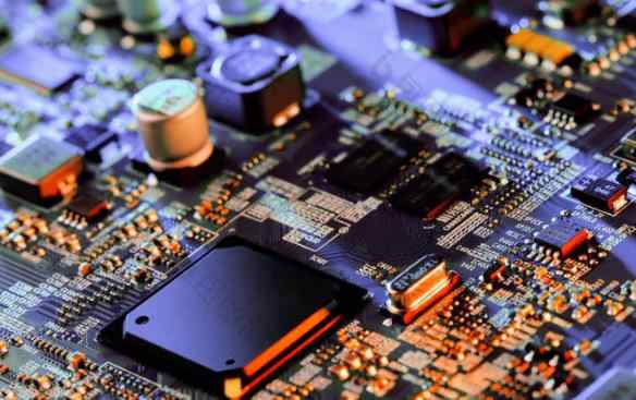
SMT projection plate, printing and wafer assembly
14 Precautions before casting and printing SMT chip processing
We are very strict in the management of SMT wafer processing process, whether it is solder paste rewarming and stirring, steel mesh scrubbing, first article verification, incoming material verification and IPQC inspection, after reaching 100% AOI test of the furnace, we are strictly in accordance with ISO9001:2008 system standards and constantly improve. Through cooperation and efforts with customers, our direct sales rate can reach more than 98%.
The PCB must be counted before being put in, and shall not be unpacked to avoid missing the original package;
2. For PCB with BGA components, 100% inspection must be carried out on the pad before input to confirm that there are no foreign matters, dirt, oxidation, etc.;
3. Do not touch PCB directly when taking PCB, especially in mobile phone products and OSP. PCB must use finger cots;
4. Set relevant printing parameters according to process requirements;
5. Add a small amount of solder paste several times, and the diameter of the solder paste rolling on the mold should be kept at 1.0-1.5cm;
7. OSP PCB must be produced within 24 hours, and excessive time will lead to serious oxidation of PCB;
8. IPQC tests the thickness of solder paste every 2 hours;
9. Before opening the line, the printing personnel need to use: wire mesh, scraper, solder paste, and special models also need to be made with clamps;
10. After production, the printer will clean the mold and scraper, and return them to the tool room together with the unused solder paste;
11. Solder paste must be preheated for 4 hours before use, and those not used for more than 24 hours must be returned to the freezer;
12. Solder paste must be mixed with a special mixer.
13. The storage conditions of solder paste are: 5-10 ℃, 6 months from the date of production;
14. The service life of solder paste added to the mold is 12 hours, and the unused life is 48 hours after the lid is opened.
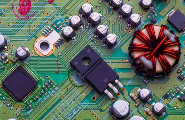
Quickly distinguish common SMT patch components
With the development of SMT chip technology, various commonly used components are becoming smaller and smaller It is difficult to distinguish chip resistor, chip inductor and chip capacitor in appearance How to quickly distinguish common SMT components? Next, the scientific and technical personnel of Jingbang Technology will introduce you the method of quick identification 1492679352965056247 [1]
1. Difference between chip inductor and chip capacitor:
(1) Look at the color (black) - usually black is a chip inductor. SMD capacitors are black and only applicable to SMD tantalum capacitors in precision equipment, while other ordinary SMD capacitors are basically not black.
(2) Please see the model code chip inductance starts from L and chip capacitance starts from C. Judging from the circle, it should be an inductor. If the resistance measured at both ends is a few tenths of an ohm, it is an inductance.
(3) The resistance of the chip inductor is generally small, and the pointer of the multimeter will not deflect back and forth due to "charging and discharging". The chip capacitor is charged and discharged.
(4) View the internal structure If the same components are found, you can fold the components to view the internal structure. The coil structure is chip inductance.
2. Differences between chip inductor and chip resistor:
(1) From the shape, the inductor is polygonal, while the resistance is basically rectangular. When the shape of the component to be identified is a polygon, especially a circle, it is usually regarded as an inductor.
(2) The measured resistance value The resistance value of the inductor is relatively small, while the resistance value of the resistor is relatively large.
3. Differences between chip capacitors and chip resistors:
(1) Look at the color chip capacitors, which are mostly gray, cyan gray and yellow, and are generally slightly lighter than the cardboard case. Some chip capacitors are not printed, mainly because they are sintered at high temperature, which makes it impossible to print on their surfaces.
(2) Look at the logo. The chip capacitor symbol in the circuit is "C", and the chip resistor symbol is "R".
(3) Generally speaking, the resistance of chip capacitor is large, while the chip resistance is relatively small. The chip capacitor is charged and discharged, but the chip resistor is not.
As long as you are familiar with various SMT components, you can quickly distinguish various components with similar appearance
14 Precautions before casting and printing SMT chip processing
We are very strict in the management of SMT wafer processing process, whether it is solder paste rewarming and stirring, steel mesh scrubbing, first article verification, incoming material verification and IPQC inspection, after reaching 100% AOI test of the furnace, we are strictly in accordance with ISO9001:2008 system standards and constantly improve. Through cooperation and efforts with customers, our direct sales rate can reach more than 98%.
The PCB must be counted before being put in, and shall not be unpacked to avoid missing the original package;
2. For PCB with BGA components, 100% inspection must be carried out on the pad before input to confirm that there are no foreign matters, dirt, oxidation, etc.;
3. Do not touch PCB directly when taking PCB, especially in mobile phone products and OSP. PCB must use finger cots;
4. Set relevant printing parameters according to process requirements;
5. Add a small amount of solder paste several times, and the diameter of the solder paste rolling on the mold should be kept at 1.0-1.5cm;
7. OSP PCB must be produced within 24 hours, and excessive time will lead to serious oxidation of PCB;
8. IPQC tests the thickness of solder paste every 2 hours;
9. Before opening the line, the printing personnel need to use: wire mesh, scraper, solder paste, and special models also need to be made with clamps;
10. After production, the printer will clean the mold and scraper, and return them to the tool room together with the unused solder paste;
11. Solder paste must be preheated for 4 hours before use, and those not used for more than 24 hours must be returned to the freezer;
12. Solder paste must be mixed with a special mixer.
13. The storage conditions of solder paste are: 5-10 ℃, 6 months from the date of production;
14. The service life of solder paste added to the mold is 12 hours, and the unused life is 48 hours after the lid is opened.
Quickly distinguish common SMT patch components
With the development of SMT chip technology, various commonly used components are becoming smaller and smaller It is difficult to distinguish chip resistor, chip inductor and chip capacitor in appearance How to quickly distinguish common SMT components? Next, the scientific and technical personnel of Jingbang Technology will introduce you the method of quick identification 1492679352965056247 [1]
1. Difference between chip inductor and chip capacitor:
(1) Look at the color (black) - usually black is a chip inductor. SMD capacitors are black and only applicable to SMD tantalum capacitors in precision equipment, while other ordinary SMD capacitors are basically not black.
(2) Please see the model code chip inductance starts from L and chip capacitance starts from C. Judging from the circle, it should be an inductor. If the resistance measured at both ends is a few tenths of an ohm, it is an inductance.
(3) The resistance of the chip inductor is generally small, and the pointer of the multimeter will not deflect back and forth due to "charging and discharging". The chip capacitor is charged and discharged.
(4) View the internal structure If the same components are found, you can fold the components to view the internal structure. The coil structure is chip inductance.
2. Differences between chip inductor and chip resistor:
(1) From the shape, the inductor is polygonal, while the resistance is basically rectangular. When the shape of the component to be identified is a polygon, especially a circle, it is usually regarded as an inductor.
(2) The measured resistance value The resistance value of the inductor is relatively small, while the resistance value of the resistor is relatively large.
3. Differences between chip capacitors and chip resistors:
(1) Look at the color chip capacitors, which are mostly gray, cyan gray and yellow, and are generally slightly lighter than the cardboard case. Some chip capacitors are not printed, mainly because they are sintered at high temperature, which makes it impossible to print on their surfaces.
(2) Look at the logo. The chip capacitor symbol in the circuit is "C", and the chip resistor symbol is "R".
(3) Generally speaking, the resistance of chip capacitor is large, while the chip resistance is relatively small. The chip capacitor is charged and discharged, but the chip resistor is not.
As long as you are familiar with various SMT components, you can quickly distinguish various components with similar appearance


Just upload Gerber files, BOM files and design files, and the KINGFORD team will provide a complete quotation within 24h.