
Professional PCB manufacturing and assembly
Building 6, Zone 3, Yuekang Road,Bao'an District, Shenzhen, China
+86-13410863085Mon.-Sat.08:00-20:00


Dyeing and penetrant testing of SMT solder joint quality
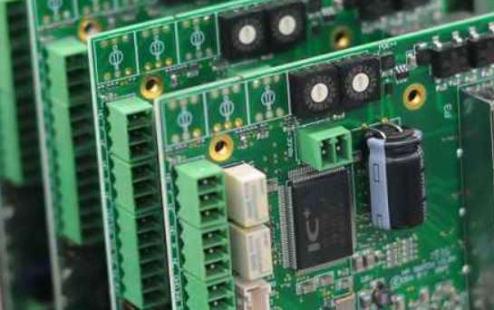
PCBA circuit board processing is an indispensable step in the process of electronic equipment design and production PCBA circuit board carries the control system of electronic equipment Its quality directly affects the operation of electronic equipment and product quality A good product cannot be separated from the support of high quality PCBA circuit board. It is inevitable to encounter some problems when dealing with PCBA circuit board With the development of surface mount technology and module high sealing technology, the quality and reliability of its solder joints have been tested. The testing technology must also meet the needs of this development New technologies using various advanced testing and testing equipment also emerge one after another, but high prices and maintenance difficulties also make most companies in the industry unable to afford
Fundamentals of Dyeing and Penetrant Testing
Put the solder joint into the red ink or dye, and let the red ink or dye penetrate into the crack of the solder joint. After drying, forcibly separate the solder joints. The weld joint usually cracks from the weak link (crack), which can be inspected. The stained area and interface at the crack point are used to judge the size and depth of the crack and the interface of the crack, so as to obtain the quality information of the solder joint.
Description of Dye and Penetrant Test Methods Sample Preparation
First, carefully cut the sample to be tested from the circuit board assembly PCBA. "If the PCBA is not big! You can also test the entire PCBA including the equipment to be tested! But to do this, you need to have a large enough red ink container, which may also waste more red ink. If the price of red ink becomes more expensive, the cost will increase." However, taking samples directly also requires special care. Special tools can be used to avoid damaging the test sample. Destruction or damage of solder joints“
Dyeing and penetration
After sample preparation, you can directly place the sample in a container filled with red ink, close it tightly, and then vacuum it. Typically, it can be pumped to a pressure of 100 mbar. Come out, let the red ink penetrate where it should go, and dye it red. In order to make the red ink have a better penetration effect, a few drops of surfactant are usually added to the red ink to reduce its surface tension
roast
The dyed sample waits for the excess red ink to drain! Place it in an oven with a temperature of about 100 ℃ and bake until the sample is dry. The time depends on the nature of the red ink used. It usually takes one hour, and the fastest time is 15 minutes! The longest drying time even exceeds one hour. "Dry samples usually need to be cooled to room temperature in a dryer to avoid moisture absorption."
Equipment separation
Dyeing equipment can be separated by various tools! In order to check whether there is a red interface at the solder joint, "the method of separation is usually to tilt the four corners of the device with an L-shaped steel hook, bend the PCBA to break the solder joint of the device", and then fix the steel cylinder of appropriate size on the device surface with a super glue (see Figure 1). After fixing the PCBA in the position of the equipment, extend the cylinder vertically to separate it.
Equipment% If the equipment is too large or rigid, the method of occupying the hole and applying force can be used, as shown in Figure 2. It is suggested to use the method of heating to 140 ℃; Or thermal insulation method, the equipment is difficult to separate! But the actual operation is very troublesome or difficult! It is rarely used in the industry.
Check and record
After separation, use a stereo microscope or metallographic microscope with sufficient magnification to check the interface of the equipment. "Please note that the separated PCB and the two surfaces of the device should be checked symmetrically. Please note that the interface dyed red should be photographed and recorded. Generally, they are symmetrical, that is, PCB. The interface between the surface and the device pin will be dyed red or not at the same time." It is specially reminded that the red interface (fault or separation mode) and area of the solder joints must be carefully recorded. The solder joints are located in all solder joints of the whole equipment Distribution law of
Analysis and Application of Dyeing and Penetration Test Results
Through the dynamic test, we can obtain information about product quality PCBA solder joints, especially the information about the separation interface and its distribution, which can provide a basis for process improvement and even distinguish the responsibility for quality accidents
Preheat PCB assembly before or during rework
Dec 06,2022


Just upload Gerber files, BOM files and design files, and the KINGFORD team will provide a complete quotation within 24h.