
Professional PCB manufacturing and assembly
Building 6, Zone 3, Yuekang Road,Bao'an District, Shenzhen, China
+86-13410863085Mon.-Sat.08:00-20:00


Introduction to SMT chip processing POP assembly process
Chip stacking technology is a new high-density assembly form developed by modern electronic information products to improve logic operation function and storage space This paper mainly analyzes and summarizes the problems and countermeasures in the realization of POP assembly process from the perspective of equipment science and technology The optimization method and scope of process parameters of main processes in POP assembly process are studied emphatically, and the problems needing attention in process control are discussed These are the keys to ensure the success rate of POP chip stacking
1 General
POP (Package on Package) is a device chip stacking technology. It is a new method of device miniaturization and high-density assembly developed to improve logic operation function and storage space.
POP technology is widely used in high-end terminal products. At present, BGA POP technology with 0.4mm spacing has the capacity of mass production.
At present, the main difficulties of BGA POP assembly process with 0.4mm spacing are:
-BGA printing solder paste and reflow soldering with lower spacing of 0.4mm are easy to bridge;
-The lower two layers are placed with high precision and easy to move;
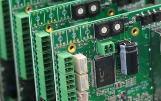
Circuit board
It is difficult to control the flux impregnation amount of the upper chip.
2 Solder paste printing
2.1 Influencing factors
Printing is a system engineering. PCB, template, solder paste and equipment work together in a certain environment according to a certain method, with many variables and complex interaction mechanisms. Summarize the main influencing factors,
The quality of solder paste printing is affected by such factors as hardware, process parameters, environment and process control. PCB and mold design, solder paste selection, process control and other problems in reliable printing of fine pitch components have been analyzed and discussed in detail in many files, and I will not repeat them here.
2.2 Support method
Common supporting casing includes "hard" casing and "soft" casing
For solder paste printing of fine pitch components, it is necessary to ensure that there is no gap between PCB and mold, and that PCB and mold are flat and not deformed during the entire printing process. It is usually wrong to think that the higher the top of the thimble, the closer the connection between PCB and mold, which helps to improve the printing quality. However, if the top of the sleeve is too high, the PCB and the mold will have a certain degree of pre deformation, as shown in Figure 4. On the one hand, the alignment between the template opening and the pad may be offset, which may cause the printing solder paste to shift; On the other hand, during the movement of the scraper, the mold and PCB will separate, resulting in uneven amount of solder paste obtained in different areas, or even insufficient amount of solder paste; At the same time, when separating templates in the printing process, the separation speed and separation distance parameters lose their meaning and are easy to sharpen.
The introduction of printing support fixture can effectively ensure the close combination of PCB and SMT mold, and the improvement of printing problems such as 0. 4mm/0.35mm spacing, soft/sheet deformation and other printing problems are obvious
2.3 Scraper
During the printing process, the solder paste should have a good rolling effect. Due to rolling, the solder paste in the front end area of the scraper will partially fill the template hole, and the flux in it will pre wet the template hole wall, which is conducive to further filling and demoulding of the subsequent solder paste, so as to obtain an ideal amount and shape of solder paste. The original "solder paste rolling column" is about 15mm in diameter. When it is reduced to half of the original size, new solder paste needs to be added. The "solder paste rolling column" shall be uniform and smooth.
In order to achieve good rolling effect, in addition to ensuring the proper viscosity and volume of solder paste, various equipment suppliers are seeking to improve the structure and working principle of the scraper. For example, DEK's vibrating scraper, ProFlow, Minami's rotary scraper, etc.
2.4 Mold cleaning frequency
On the premise that the bottom of the wire mesh is clean, the cleaning frequency of the wire mesh shall be minimized. There are burrs of various sizes on the steel mesh wall processed by cutting method, which hinder the filling and demoulding of solder paste. In the normal printing process, the wall of the wire mesh will be wetted by the flux, and various forces will reach a balanced state. During the cleaning process, due to the effect of alcohol and vacuum, the flux wetted film is damaged and the burrs are exposed again. Only after a few printing cycles can a new balance be established. This is why the tin content of the mould cleaned in production will decrease when it is printed for the first time.
Too frequent cleaning may also cause the solvent to mix into the solder paste and affect the viscosity of the solder paste; The solvent volatilization will affect the optimal working temperature of solder paste and mold, and destroy the system balance.
3 Patch
Compared with traditional components, the key problem in POP placement is to realize and control the dipping effect of flux (solder paste) and ensure the placement accuracy of BGA.
3.1 Patch Mode
Fuji NXT/AIM equipment has three POP placement modes:
-Absorption equipment - image recognition - immersion flux patch;
-µ Absorption device - image recognition - immersion flux - image recognition - patch;
-Pick up the device - Immersion flux - Image recognition - Patch.
In the import phase, two kinds of flux were selected for comparative testing, namely blue flux and colorless flux.
-After the equipment is immersed in blue flux, image recognition cannot be performed, so only the first patch mode can be used;
White flux will not affect image recognition. The second or third patch mode can be used.
White light flux and second patch mode are recommended.
3.2 Impregnating flux (solder paste)
Fuji flux unit can realize automatic supply of flux (solder paste) and automatic thickness control.
The introduction of the new process proved that the effect of using flux was better than that of using solder paste. The thickness of the flux shall be adjusted according to the spacing value of the lower wafer solder balls, and the wetting shall be greater than 50% of the height of the solder balls. The wetted surface requires a horizontal surface. Generally, the 0.4 mm spacing PoP is adjusted to (0.19 0.20) mm, and the 0.5 mm spacing is adjusted to (0.19 0.23) mm. The thickness of the flux is adjusted by the gauge attached to the equipment.
3.3 Image recognition
Fuji chip mounter has two digital cameras. One reads PCB marking information and calculates the marking center to locate PCB The other reads the key information of the device pin (solver ball), which calculates the main body and other key information of the central location of the device, so as to install the device to the corresponding location in the program


Just upload Gerber files, BOM files and design files, and the KINGFORD team will provide a complete quotation within 24h.