
Professional PCB manufacturing and assembly
Building 6, Zone 3, Yuekang Road,Bao'an District, Shenzhen, China
+86-13410863085Mon.-Sat.08:00-20:00

EMI Solution for Multilayer PCB Design
There are many ways to solve the problem of electromagnetic interference. Modern EMI suppression methods include: using EMI suppression coating, selecting appropriate EMI suppression spare parts, EMI simulation design, etc. Starting from the basic PCB layout, this paper discusses the function and design technology of PCB stack in EMI radiation control.
Power bus bar of printed circuit board
A reasonable capacitor placed near the IC pin can make the IC output voltage jump quickly. However, this is not the end of the problem. Due to the limited frequency response of the capacitor, it is impossible for the capacitor to generate the harmonic power required to drive the IC output cleanly in the full frequency band. In addition, the transient voltage formed at the power confluence generates voltage drop at both ends of the inductor in the decoupling path, which is the main common mode EMI interference source. How should we solve these problems?
There are many ways to solve the problem of electromagnetic interference. Modern EMI suppression methods include: using EMI suppression coating, selecting appropriate EMI suppression spare parts, EMI simulation design, etc. Starting from the basic PCB layout, this paper discusses the function and design technology of PCB stack in EMI radiation control.
Power busbar
A reasonable capacitor placed near the IC pin can make the IC output voltage jump quickly. However, this is not the end of the problem. Due to the limited frequency response of the capacitor, it is impossible for the capacitor to generate the harmonic power required to drive the IC output cleanly in the full frequency band. In addition, the transient voltage formed at the power confluence generates voltage drop at both ends of the inductor in the decoupling path, which is the main common mode EMI interference source. How should we solve these problems?
For the integrated circuit on our printed circuit board, the power layer around the integrated circuit can be regarded as a good high-frequency capacitor, which can collect part of the energy leaked from the discrete capacitor. These capacitors provide high-frequency energy to achieve clean output. In addition, the inductance of the good power layer is small, and the transient signal synthesized by the inductor is small, thus reducing the common mode electromagnetic interference.
Of course, the connection between the power supply layer of the printed circuit board and the IC power supply pin must be as short as possible, because the digital signal rises faster and faster. It is better to go directly to the bonding pad where the IC power supply pin is located, which will be discussed separately.
In order to control common mode EMI, the power layer must be a pair of well-designed power layers to help decoupling and have a sufficiently low inductance. Some people may ask, how good is this? The answer to the question depends on the power layer, inter layer data, and operating frequency (i.e., a function of IC rise time). Generally, the gap between the power layers is 6 mil, and 3 Meiji is FR4 data. The equivalent capacitance of the power layer is about 75pF per square inch. Obviously, the smaller the layer spacing, the greater the capacitance.
There are not many devices with a rise time between 100 and 300 ps, but according to the current development speed of integrated circuits, devices with a rise time between 100 and 300 ps will account for a large proportion. For circuits with rise times of 100 to 300 PS, 3 3mil layer spacing is no longer appropriate for most applications. At that time, it was necessary to use layer technology with layer spacing less than 1 mil and replace FR4 dielectric material with high dielectric constant data. Today, ceramics and ceramic plastics can meet the design requirements of 100 to 300 PS rise time circuits.
Although new materials and methods may be introduced in the future, common mode EMI may be very low for today's common 1 to 3 ns rise time circuits, 3 to 6 mil layer spacing, and FR4 dielectric data, which are usually sufficient to handle high-end harmonics and keep transient signals at a sufficiently low level. The PCB stack design example given in this paper assumes that the layer spacing is 3 to 6 mils.
PCB electromagnetic mask
From the perspective of signal routing, a good layering strategy should be to place all signal routes on one or more layers, which are close to the power layer or ground plane. For power supply, a good layering strategy should be that the power layer is adjacent to the ground layer, and the distance between the power layer and the ground layer should be as small as possible. This is what we call a "tiered" strategy.
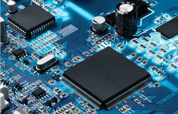
Printed circuit board
PCB stacking
What stacking strategies can help mask and suppress EMI? The following layered superposition scheme assumes that the power current flows on a single layer and that a single voltage or multiple voltages are distributed in different parts of the same layer. The case of multiple power layers will be discussed later.
4-layer printed circuit board
There are several potential problems in the 4-floor design. First of all, even if the signal layer is outside and the power layer and the ground plane are inside, the gap between the power layer and the ground plane is too large.
If the cost requirement is the first, consider the following two methods to replace the traditional 4-layer board. Both can improve EMI suppression efficiency, but only when the component density on the circuit board is low enough and there is enough area around the component to place the required copper clad power supply.
The first is the preferred solution, in which the outer layer of the printed circuit board is a layer and the middle layer is a signal/power layer. The power supply on the signal layer is connected through wide lines, which makes the path impedance of power current low and that of signal microstrip low. From the perspective of EMI control, this is the best four layer PCB structure available. The second scheme uses the outer and middle layers to traverse the signal. Compared with the traditional 4-layer plate, the improvement is small, and the interlayer impedance is as poor as the traditional 4-layer plate.
If the line impedance is to be controlled, the above stacking scheme will carefully place the line under the power and grounding copper island. In addition, copper islands on the power supply or stratum shall be interconnected as closely as possible to ensure DC and low-frequency connections.
6-layer printed circuit board
If the component density on the 4-layer panel is high, it is better to use the 6-layer panel. However, some stacking schemes in the 6-layer panel design do not cover the electromagnetic field well, and have little effect on reducing the transient signal of the power bus. Two examples are discussed below.
In the first example, the power supply and ground are placed on the second and fifth layers respectively. Because of the high copper clad impedance of the power supply, this is very unfavorable to the control of common mode EMI radiation. However, from the point of view of signal impedance control, this method is very correct.
In the second example, the power and ground are placed on the third and fourth layers respectively. This design solves the problem of copper clad impedance of power supply. Due to the poor effectiveness of the electromagnetic masks on the first and sixth layers, differential mode EMI is added. If the number of signal lines on the two outer layers is the smallest, the line length is very short (less than 1/20 of the maximum harmonic wavelength of the signal). The design solves the problem of differential mode electromagnetic interference. The differential mode EMI can be well suppressed by laying copper in the external non component and non wiring areas and grounding the copper clad areas (once every twenty wavelengths). As previously mentioned, the copper laying area should be associated with multiple points of the internal ground plane.
The general high-performance 6-layer design usually lays the first and sixth layers into the stratum, and the third and fourth layers are energized and grounded. EMI suppression effect is good because there are two layers of central double microstrip signal lines between the power layer and adjacent layers. The disadvantage of this design is that there are only two layers in the line layer. As mentioned earlier, if the outer layer is short and copper is laid in the wireless area, the traditional 6 is used. Layers can also achieve the same stacking.
Another 6-layer layout is signal, grounding, signal, power supply, grounding, and signal, which can realize the environment required for advanced signal integrity design. The signal layer is adjacent to the ground layer, and the power layer is paired with the interface layer. Obviously, the disadvantage is that the layers are stacked unevenly.
This usually leads to problems in processing and manufacturing. The solution is to fill all blank areas in layer 3 with copper. If the copper density of layer 3 is close to the power layer or ground plane, it can be loosely regarded as a circuit board with balanced structure. The copper filled area must be connected to power or ground. The distance between the connecting holes is still 1/20 of the wavelength and is not always connected anywhere. Connect, but preferably connect.
10 layer printed circuit board
Because the insulation isolation layer between layers is very thin, and the impedance between layers 10 or 12 of the circuit board and each layer is very low, as long as there is no fault in each layer and stack, good signal integrity can be expected. It is more difficult to process 12 layers with a thickness of 62mil, and fewer manufacturers can process 12 layers.
Because there is always an insulating layer between the signal layer and the loop layer, it is not optimal to assign 6 layers in the middle of the 10 layer design to take the signal line. In addition, it is important to make the signal layer adjacent to the loop layer, that is, the layout of the circuit board is signal, grounding, signal, signal, grounding, and signal.
This design provides a good path for signal current and its loop current. The proper cabling strategy is that the first layer follows the X direction, the third layer follows the Y direction, the fourth layer follows the X direction, and so on. Visually, the first and third layers are a pair of layers, the fourth and seventh layers are a pair of layers, and the eighth and tenth layers are the last pair of layers. When it is necessary to change the line direction, the signal line on the first layer shall change the direction after the third layer through the "through hole". In fact, this may not always be possible, but it should be observed as a design concept as much as possible.
Similarly, when the signal direction changes, the signal shall be routed from layer 8 and layer 10 or layer 4 to layer 7 through the hole. This wiring ensures the closest coupling between the signal forward path and the loop. For example, if the signal is on the first layer and the loop is on the second layer and only on the second layer, then even if the signal on the first layer is transferred to the third layer through the "hole", the circuit is still on the second layer, which maintains the characteristics of low inductance, large capacitance and good electromagnetic shielding efficiency.
What if not? For example, the signal line on the first layer passes through the hole to reach the tenth layer, and then the loop signal must find the ground plane from the ninth layer, and the loop current needs to find the nearest ground through the hole (such as the grounding pin of resistor or capacitor). If there is such a hole nearby, it is really lucky. If there is no such near hole, the inductance will increase, the capacitance will decrease, and the electromagnetic interference will increase.
When the signal wire must leave the current layer pair in other layers through the hole, the grounding hole should be placed close to the hole so that the loop signal can be returned to the appropriate connection layer smoothly. For layers 4 and 7, the signal loop will return from the power layer or ground layer (i.e. layer 5 or 6), because the capacitive coupling between the power layer and the interface layer is good, and the signal is easy to transmit.
Multi power layer design
If two power layers of the same voltage source need to output large current, the circuit board shall be arranged in two groups of power layers and connection layers. In this case, an insulating layer is placed between each pair of power layers and the connecting layer. As expected, this will result in two pairs of equal impedance power flows. If the stacking of power layers leads to unequal impedance, the shunt will be uneven. The transient voltage is much larger, and the electromagnetic interference increases sharply.
If there are multiple power supply voltages with different values on the circuit board, multiple power layers are required accordingly. Remember that each pair of power layers and connection layers are created for different power supplies. In both cases, remember the manufacturer's requirements for a balanced structure when determining the position of the paired power and connection layers on the circuit board.
Summary
Because the thickness of PCB designed by most engineers is 62mil, there is no blind hole or buried hole. The discussion on layering and stacking of PCB is limited to this The layering scheme recommended in this paper may not be suitable for circuit boards with large thickness differences In addition, the delamination method proposed in this paper is not applicable due to the different processing technologies of blind hole or buried hole printed circuit boards
Introduction to PCB Cleanliness Control
Dec 06,2022


Just upload Gerber files, BOM files and design files, and the KINGFORD team will provide a complete quotation within 24h.