
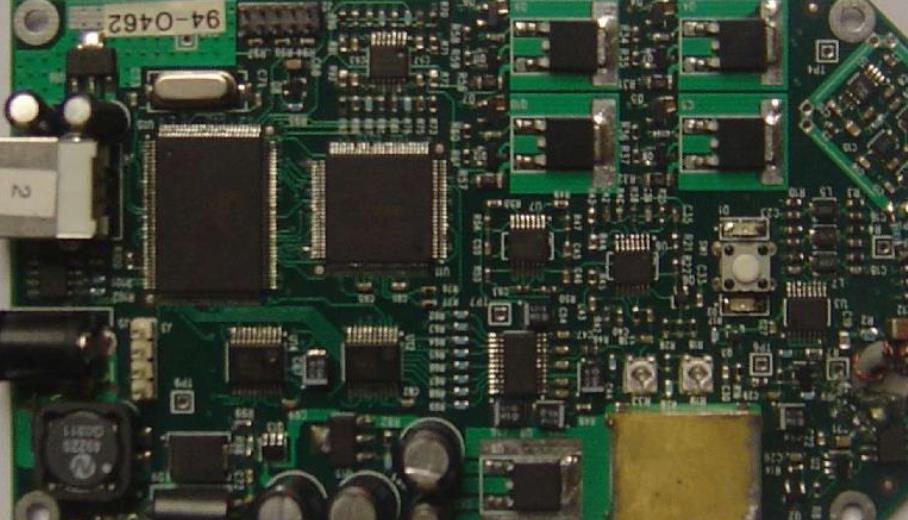
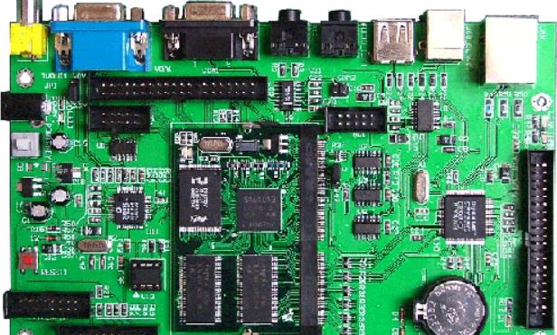
Professional PCB manufacturing and assembly
Building 6, Zone 3, Yuekang Road,Bao'an District, Shenzhen, China
+86-13410863085Mon.-Sat.08:00-20:00

Surface mount technology accelerates electronic assembly and red glue process
SMT accelerates the efficiency of electronic assembly
In today's society, the electronic manufacturing industry has developed very rapidly, and the SMT processing technology has also made great progress. In this case, why is patch operation an inevitable part of the company's manufacturing plant? How does SMT chip processing chip technology improve the efficiency of electronic assembly? This article will answer for you.
In today's society, the electronic manufacturing industry is developing very rapidly, and the chip processing technology has also been greatly improved In this case, why is the placement operation an inevitable part of the manufacturing in the company's production plant? How does SMT chip processing chip technology improve electronic assembly efficiency? This article will answer for you
1. Microchip Processing Technology
Some precision processing technologies used in micro/nano chip processing, microchip processing and electronic manufacturing are collectively referred to as microchip processing.
2. Interconnection Packaging Technology
Interconnection between the wafer and the outgoing circuit on the substrate, such as flip chip bonding, wire bonding, silicon through hole (TSV), and packaging technology after the wafer and the substrate are interconnected. This technology is often referred to as chip packaging technology. Passive component manufacturing technology. Including the manufacturing technology of passive components, such as capacitors, resistors, inductors, transformers, filters and antennas.
3. Photoelectric packaging technology
Optoelectronic packaging is the systematic integration of optoelectronic devices, electronic components and functional application data. In the optical communication system, optoelectronic packaging can be divided into chip integrated circuit level packaging, device packaging and die MEMS manufacturing technology. A micro system that uses microchip processing technology to integrate sensors, actuators, and processing control circuits on a single silicon chip.
4. Electronic assembly technology
Electronic assembly technology is often called board level packaging technology. Electronic assembly technology is mainly surface assembly and through hole insertion technology. Electronic material technology. Electronic materials refer to materials used in electronic technology and microelectronic technology, including dielectric materials, semiconductor devices, piezoelectric and ferroelectric materials, conductive metals and their alloys, magnetic materials, optoelectronic materials, electromagnetic wave mask materials and other relevant materials. The preparation and application of electronic materials are the basis of electronic manufacturing technology.
SMT patch red glue process and process description
There are two processes for SMT to process the red adhesive film One is through a needle tube The amount of SMT red glue varies according to the size of the components Manually click the SMT red glue applicator, control the glue application time, and automatically click the SMT red glue applicator Control point SMT red glue machine passes through different glue ports and glue time; The other is printing glue, SMT red glue is printed through SMT steel mesh, and SMT steel mesh meets the standard size
There are two processes for the processing of smt patch red glue film. One is through a needle tube. According to the size of the components, the amount of smt red glue is different. Manually click the time of the smt red glue machine to control the amount of glue, and automatically click the control point of the smt red glue machine. The smt red glue machine passes through different glue ports and glue times; The other is printing glue. SMT red glue is printed through SMT screen, and SMT screen meets the standard size.
PCB chip processing customization
SMT red film processing is generally aimed at power board processing, because SMT red film processing products require SMT patch components larger than 0603 for mass production.
At present, there is also a process called dual process in the SMT chip processing industry. It is also SMT patch red and solder paste technology. Solder paste after printing, then red glue. Or open the SMT step template and print the red glue. This process is used when tin dipping is required, but it is now very mature when most smd components are produced on PCBA boards.
PCB chip processing customization
Common Problems and Solutions in SMT Red Film Processing
Common problems of SMT red adhesive:
1. Insufficient power
The reasons for insufficient thrust are: 1. Insufficient glue consumption 2. The colloid is not completely solidified 3. PCB board or component is polluted 4. The colloid itself is very fragile and has no strength
2. Insufficient glue or leakage
Reasons and counter measures: 1. The printing plate is not cleaned frequently, and it is cleaned with ethanol every 8 hours 2. There are impurities in the colloid 3. The opening of filter screen is unreasonable or the point air pressure is too small There are bubbles in the colloid 5. If the rubber head is closed, it should be cleaned immediately 6. Preheating temperature of dispensing head is not enough, and the temperature of dispensing head should be set to 38 ℃
PCB chip processing customization
3 Lars
The so-called wire drawing means that the adhesive film will not break during the SMT dispensing process, and the movement direction from the adhesive film to the adhesive head is a filament connection phenomenon. There are many circuits and the film is covered on the printed board, which will lead to poor welding. Especially when large size is used, the tip of the mouth is more prone to this phenomenon. The main components of SMT adhesive are the tensile efficiency of resin and the setting of coating conditions.
Solution:
1. Reduce traffic
2. The lower the viscosity is, the higher the contact degree is, and the lower the tensile tendency is, so we should choose as many adhesives as possible.
3. The temperature of the temperature regulator is slightly higher, and the adhesive must be adjusted to low viscosity and high contact film
SMT accelerates the efficiency of electronic assembly
In today's society, the electronic manufacturing industry has developed very rapidly, and the SMT processing technology has also made great progress. In this case, why is patch operation an inevitable part of the company's manufacturing plant? How does SMT chip processing chip technology improve the efficiency of electronic assembly? This article will answer for you.
In today's society, the electronic manufacturing industry is developing very rapidly, and the chip processing technology has also been greatly improved In this case, why is the placement operation an inevitable part of the manufacturing in the company's production plant? How does SMT chip processing chip technology improve electronic assembly efficiency? This article will answer for you
1. Microchip Processing Technology
Some precision processing technologies used in micro/nano chip processing, microchip processing and electronic manufacturing are collectively referred to as microchip processing.

2. Interconnection Packaging Technology
Interconnection between the wafer and the outgoing circuit on the substrate, such as flip chip bonding, wire bonding, silicon through hole (TSV), and packaging technology after the wafer and the substrate are interconnected. This technology is often referred to as chip packaging technology. Passive component manufacturing technology. Including the manufacturing technology of passive components, such as capacitors, resistors, inductors, transformers, filters and antennas.
3. Photoelectric packaging technology
Optoelectronic packaging is the systematic integration of optoelectronic devices, electronic components and functional application data. In the optical communication system, optoelectronic packaging can be divided into chip integrated circuit level packaging, device packaging and die MEMS manufacturing technology. A micro system that uses microchip processing technology to integrate sensors, actuators, and processing control circuits on a single silicon chip.
4. Electronic assembly technology
Electronic assembly technology is often called board level packaging technology. Electronic assembly technology is mainly surface assembly and through hole insertion technology. Electronic material technology. Electronic materials refer to materials used in electronic technology and microelectronic technology, including dielectric materials, semiconductor devices, piezoelectric and ferroelectric materials, conductive metals and their alloys, magnetic materials, optoelectronic materials, electromagnetic wave mask materials and other relevant materials. The preparation and application of electronic materials are the basis of electronic manufacturing technology.
SMT patch red glue process and process description
There are two processes for SMT to process the red adhesive film One is through a needle tube The amount of SMT red glue varies according to the size of the components Manually click the SMT red glue applicator, control the glue application time, and automatically click the SMT red glue applicator Control point SMT red glue machine passes through different glue ports and glue time; The other is printing glue, SMT red glue is printed through SMT steel mesh, and SMT steel mesh meets the standard size
There are two processes for the processing of smt patch red glue film. One is through a needle tube. According to the size of the components, the amount of smt red glue is different. Manually click the time of the smt red glue machine to control the amount of glue, and automatically click the control point of the smt red glue machine. The smt red glue machine passes through different glue ports and glue times; The other is printing glue. SMT red glue is printed through SMT screen, and SMT screen meets the standard size.
PCB chip processing customization
SMT red film processing is generally aimed at power board processing, because SMT red film processing products require SMT patch components larger than 0603 for mass production.
At present, there is also a process called dual process in the SMT chip processing industry. It is also SMT patch red and solder paste technology. Solder paste after printing, then red glue. Or open the SMT step template and print the red glue. This process is used when tin dipping is required, but it is now very mature when most smd components are produced on PCBA boards.
PCB chip processing customization
Common Problems and Solutions in SMT Red Film Processing
Common problems of SMT red adhesive:
1. Insufficient power
The reasons for insufficient thrust are: 1. Insufficient glue consumption 2. The colloid is not completely solidified 3. PCB board or component is polluted 4. The colloid itself is very fragile and has no strength
2. Insufficient glue or leakage
Reasons and counter measures: 1. The printing plate is not cleaned frequently, and it is cleaned with ethanol every 8 hours 2. There are impurities in the colloid 3. The opening of filter screen is unreasonable or the point air pressure is too small There are bubbles in the colloid 5. If the rubber head is closed, it should be cleaned immediately 6. Preheating temperature of dispensing head is not enough, and the temperature of dispensing head should be set to 38 ℃
PCB chip processing customization
3 Lars
The so-called wire drawing means that the adhesive film will not break during the SMT dispensing process, and the movement direction from the adhesive film to the adhesive head is a filament connection phenomenon. There are many circuits and the film is covered on the printed board, which will lead to poor welding. Especially when large size is used, the tip of the mouth is more prone to this phenomenon. The main components of SMT adhesive are the tensile efficiency of resin and the setting of coating conditions.
Solution:
1. Reduce traffic
2. The lower the viscosity is, the higher the contact degree is, and the lower the tensile tendency is, so we should choose as many adhesives as possible.
3. The temperature of the temperature regulator is slightly higher, and the adhesive must be adjusted to low viscosity and high contact film


Just upload Gerber files, BOM files and design files, and the KINGFORD team will provide a complete quotation within 24h.