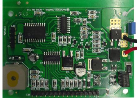
On line Testing in Smt Patch Processing
SMT chip processing is not only to place components on designated PCB pads If you want to gain good quality and customer reputation, obviously, this is not enough Sufficient data must be obtained through various test methods to obtain specific test data and records that support quality requirements At this time, various detection technologies and methods become very important
Today, I will discuss issues related to online testing (ICT) from the perspective of smt processing plants. On line testing (ICT) is usually used to detect the direction of a circuit board, such as open circuit, resistance, capacitance and components, but it is also a relatively less used device. What are the specific advantages and disadvantages?
ICT test
As we all know, online testing or ICT works by using a set of probes to access circuit nodes and then checking the performance of each component. It can also test the function of digital circuits, but the cost involved is very high.
Circuit board

In general, the advantage of ICT is the need to test a large number of products It can also be used to test well developed products However, because ICT needs to create custom devices, the cost and lead time involved are high However, the advantage of ICT is that once you prepare the customized tools, the organizational cost will be very low, but the cost of PCB processing in small batches is obviously high
If we summarize the advantages and disadvantages of ICT, they will be as follows:
Advantages:
1. Helps to quickly test each PCBA unit.
2. Low organizational costs.
3. You can test individual components.
4. It works well when you need to test logical functionality.
5. Can be used to test LED components.
6. You can use it to test the welding of BTC components by stress testing.
Disadvantages:
1. The lead time required for development is usually very long, which may be a problem in today's era when fast time to market becomes a source of competitive advantage.
2. High upfront costs may be detrimental to its use.
3. Programming tools are required.
4. It cannot be used to test non electric components or connectors.
5. Although it can be used to test individual components, it is not suitable for testing components that work together.
Mistakes in selecting smt wafer processing plants
Myth 1: Large companies will charge lower appreciation profit margins
Similarly, although this may sometimes be true, it is not a universal premise. This is because, although large electronic contract manufacturers may receive volume discounts on raw material demand, labor costs may or may not follow the same approach. In this case, the price of large SMT processing plants is not necessarily low, and the price of small plants is not necessarily high.
Myth 2: If the manufacturer has a good vertical integration model, it can provide a lower price
This is not always given. Some electronic contract manufacturers can do this, and some may not have the corresponding strength. The supply chain will be unstable at any time, but the factory that can implement the vertical integration mode may be more powerful than other companies, and can also provide you with competitive prices.
Myth 3: Electronic contract manufacturers should not work for my competitors
Your fears may be completely unfounded As long as the electronic contract manufacturer is compatible with your overall project and cooperates with your competitors, this should not affect the cooperation between both parties Professional contract manufacturers will be fully aware of PCB manufacturing process This is also a necessary confidential quality for long-term suppliers


