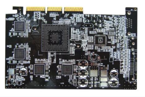
What is a PCB stack? What should I pay attention to?
What is a PCB stack and does your application need it? How does the PCB stack work? Here are some PCB stack basics to help you solve all problems.
All about PCB layer stacking
Pcba processing layering or stacking is just a method to obtain multiple printed circuit boards in the same device by stacking them together while ensuring that there are predefined interconnections between them. These multilayer PCBs can increase speed and function in the device, and are composed of at least three conductive layers, with the bottom layer combined with the insulating board.
Although PCB stacking can bring many advantages, including reducing impedance mismatch and signal crosstalk, there are also challenges in pcba production of circuit layer stacking.
Some problems with PCB multilayer stacking may include:
Increased EMI radiation: If the stack is poorly designed and there is an impedance mismatch, reflection will occur in the system, which may occur. Proper stacking design will reduce mismatch and prevent this problem.

Interlayer offset: If you encounter problems with interlayer offset, the use of hot-melt and rivet and pin methods for panel side design should prevent it from occurring in the future.
If white spots appear when pcba chip processing plants stack circuit boards, please add silicon pads with epoxy resin boards when arranging circuit boards. This will balance the pressure and eliminate pitting while maintaining a uniform plate thickness.
Other PCB stacking precautions
The multilayer PCB stack should strive to meet the following five objectives:
The ground plane and the power layer shall be coupled as closely as possible.
The signal layer is always adjacent to the plane.
The signal layers are coupled to their planes as closely as possible.
High speed signals are routed through buried layers between planes to contain radiation.
Multiple ground planes to reduce impedance and radiation Not every PCB stack needs to meet all of these goals. In fact, pcba board manufacturers will need an eight layer board to cover all five layers. However, you should try to achieve as many goals as possible in your stack design, and work with your PCB engineering team to determine which of these goals is the highest priority for boards with less than eight layers.


