

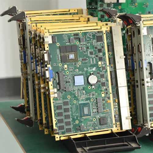
Small batch PCB assembly patch
Name: Small batch PCB assembly patch
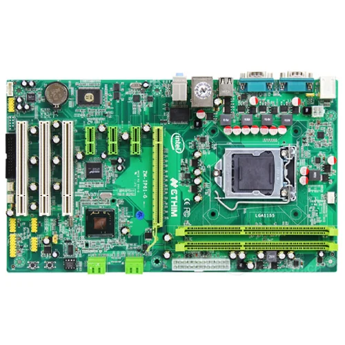
Substrate: FR-4/High TG/Polyimild/PTFE/Rogers
Copper Thickness: 1/3OZ- 6OZ
Plate thickness: 0.21-6.0mm
minute. Hole size: 0.20mm
minute. Line width: 4 million
minute. Line spacing: 0.075 mm
Surface treatment: spray tin/gold drill/OSP/lead-free spray tin
Board size: minimum 10*15mm, maximum 508*889mm
Product Type: OEM&ODM
PCB standard: IPC-A-610 D/IPC-III standard
Certificate: ISO9001/ CE//TUV/ ROHS
Warranty: 1 year
Service: One-stop turnkey service
Electronic testing: 100%
Logistics: Air/Sea
For SMT small-batch patch processing, there are many factors to be considered in pcb wiring. In actual production, the effect cannot be achieved simply by using automatic wiring tools. This is not only related to PCB production costs, electromagnetic interference between components, and appearance. Many factors such as aesthetics will also affect the effect of SMT chip processing.
Although there is no uniform standard among different boards, there are some generally applicable principles in SMT patch proofing:
1. For double-sided or multi-layer boards, the lines on both sides of the circuit board should be perpendicular to each other to prevent crosstalk caused by mutual induction.
2. Wiring priority: key signal lines are prioritized, such as power supply, analog small signal, high-speed signal, clock signal and synchronization signal.
3. If there are high-current devices on the pcb board, such as relays, indicator lights and speakers, it is best to separate the ground wires to reduce noise on the ground wires.
4. If there is a small signal amplifier on the circuit board of the smt patch processing factory, the weak signal line before amplification should be far away from the strong signal line, and the wiring must be as short as possible, and if possible, it should be shielded with a ground wire .
5. In order to reduce the interference of the board, the smt electronics factory should leave a large gap between the parallel signal lines. If there are two signal lines that are close to each other, it is best to run a grounding line between the two lines, which can play a shielding role. The distance between the high-voltage signal lines needs to consider the requirements of the insulation resistance and breakdown voltage between the wires under the worst conditions.
6. When designing the signal transmission line of the SMT patch proofing line, it is necessary to avoid excessive steering angles, so as to prevent reflections due to sudden changes in the characteristic impedance of the transmission line. It can be considered to design a uniform arc line or obtuse angle with a certain size. In addition, at the sharp outer corner, the copper foil is easy to peel off or warp.
PCBA small-batch proofing has requirements for the component layout of SMT patch processing. Reasonable layout planning will play a role in the process of processing and production. If the layout problem is arbitrary and does not consider the actual processing situation, it will cause certain troubles in production. , and the layout requirements of different processing methods are different. Components are the components of small machines and instruments, which are often composed of several parts and can be used in similar products; often refer to certain parts in industries such as electrical appliances, radios, and instruments, such as capacitors, transistors, hairsprings, springs Wait. Mainly divided into: antivirus components, electronic components, pneumatic components, Hall components, etc. A component is a graphic, button or a small animation that can be taken out repeatedly. The small animation in the component can be played independently of the main animation. Each component can be composed of multiple independent elements. Many commercial computer-aided engineering (CAE) software design packages are capable of modeling heat flow through an RF/microwave circuit, including the thermal conductivity of a PCB, at a given applied power level and given circuit parameter settings.

PCB Layout requirements for SMT patch components for Pcba small batch proofing.
1. Replaceable and adjustable components If you encounter components and parts that need to be replaced or adjusted frequently, you need to consider the characteristics and requirements of the entire machine and place them in a position that is easy to replace.
2. During the mounting process of temperature-sensitive components, if you encounter temperature-sensitive components, you must stay away from heating components, such as triodes, integrated circuits, electrolytic capacitors, etc., and keep away from high-power components and radiators. and high power resistors.
3. Arrangement direction In the actual processing of pcba small batch proofing, the arrangement direction of SMD components is also required. Try to keep the same direction, and the feature direction should be consistent, which is convenient for subsequent mounting, welding and testing, especially The printing direction of the number of components must be the same.
4. Balanced distribution SMT components with higher quality will have a larger heat capacity than ordinary components during reflow soldering processing, which will lead to local temperature differences and even virtual soldering problems. Keep the distribution balanced in SMT SMT processing This type of problem can be avoided, and the balance of the circuit board can also be maintained.
5. Heating components When different components come into contact with each other, it will affect other components, such as heating components, which are generally placed in corners and ventilation positions to facilitate heat dissipation. The heating element must be supported by other leads or supports, and a certain distance should be kept from the surface of the printed circuit board, the minimum should not be less than 2mm, otherwise the quality of the circuit board will be affected.
Kingford supports Small batch PCB assembly patch business, we are a professional PCBA one-stop assembly factory, welcome to place an order.
Name: Small batch PCB assembly patch
Substrate: FR-4/High TG/Polyimild/PTFE/Rogers
Copper Thickness: 1/3OZ- 6OZ
Plate thickness: 0.21-6.0mm
minute. Hole size: 0.20mm
minute. Line width: 4 million
minute. Line spacing: 0.075 mm
Surface treatment: spray tin/gold drill/OSP/lead-free spray tin
Board size: minimum 10*15mm, maximum 508*889mm
Product Type: OEM&ODM
PCB standard: IPC-A-610 D/IPC-III standard
Certificate: ISO9001/ CE//TUV/ ROHS
Warranty: 1 year
Service: One-stop turnkey service
Electronic testing: 100%
Logistics: Air/Sea
