
Professional PCB manufacturing and assembly
Building 6, Zone 3, Yuekang Road,Bao'an District, Shenzhen, China
+86-13410863085Mon.-Sat.08:00-20:00

1、 What is an HDI board?
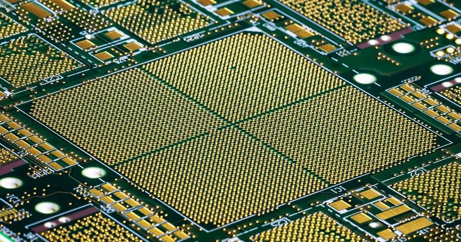
HDI board (High Density Interconnector), namely high-density interconnection board, is a circuit board with high circuit distribution density using micro blind hole embedding technology. The HDI board has an inner layer circuit and an outer layer circuit, and then uses drilling, hole metallization and other processes to connect the internal circuits of each layer.
pcba
2、 Difference between HDI board and common pcb
HDI boards are generally manufactured by lamination method. The more times of lamination, the higher the technical level of boards. Ordinary HDI boards are basically stacked once, while high-order HDI boards are stacked twice or more, and advanced PCB technologies such as hole stacking, electroplating and hole filling, and laser direct drilling are also used. When the density of PCB is increased to more than eight layers, the cost of HDI manufacturing will be lower than that of traditional complex pressing process.
HDI board has higher electrical performance and signal correctness than traditional PCB. In addition, HDI board has better improvement for radio frequency interference, electromagnetic wave interference, electrostatic discharge, heat conduction, etc. High density integration (HDI) technology can make the terminal product design smaller, while meeting higher standards of electronic performance and efficiency.
HDI boards are plated with blind holes for secondary pressing, including first, second, third, fourth and fifth steps. The first level is relatively simple, and the process and process are easy to control. The main problems of the second order are: first, alignment, and second, punching and copper plating. There are many kinds of second order designs. One is stagger position of each order. When it is necessary to connect the next adjacent layer, it is connected in the middle layer through wires, which is equivalent to two first order HDIs. The second is that the two first order holes overlap, and the second order is realized by overlapping. The processing is similar to the two first order holes, but there are many process points to be specially controlled, that is, the above mentioned. The third method is to directly drill from the outer layer to the third layer (or N-2 layer). The process is different from the previous one, and the drilling is more difficult. For the third order, the second order analogy is.
In PCB proofing, HDI costs a lot, so most PCB proofing manufacturers are unwilling to do it. Jieduobang can do HDI blind buried PCB boards that others do not want to do. At the present stage, the HDI technology adopted by JETDO has broken through the highest number of layers, which is 20; The order of blind hole is 1-4; The minimum hole diameter is 0.076mm, and the process is laser drilling.
3、 Advantages of HDI board
This kind of PCB has developed rapidly on the basis of highlighting its advantages:
1. HDI technology helps to reduce PCB cost;
2. HDI technology increases the linear density;
3. HDI technology is conducive to the use of advanced packaging;
4. HDI technology has better electrical performance and signal effectiveness;
5. HDI technology has better reliability;
6. HDI technology is better in heat dissipation;
7. HDI technology can improve RFI (radio frequency interference)/EMI (electromagnetic interference)/ESD (electrostatic discharge);
8. HDI technology improves design efficiency;
4、 HDI board material
There are some new requirements for HDI PCB materials, including better dimensional stability, anti-static mobility and non adhesive. The typical material of HDI PCB is RCC (resin coated copper). There are three types of RCC, namely polyimide metallized film, pure polyimide film and cast polyimide film.
The advantages of RCC include: small thickness, light weight, flexibility and flammability, compatibility characteristic impedance and excellent dimensional stability. In the process of HDI multilayer PCB, it replaces the traditional adhesive sheet and copper foil as the insulating medium and conductive layer, and can suppress RCC with chips through the traditional suppression technology. Non mechanical drilling methods such as lasers are then used to form micro via interconnects.
RCC promotes the occurrence and development of PCB products from SMT (surface mount technology) to CSP (chip level packaging), from mechanical drilling to laser drilling, and promotes the development and progress of PCB micro through-hole, all of which become the leading HDI PCB materials of RCC.
In the actual PCB manufacturing process, for the selection of RCC, there are usually FR-4 standard Tg 140C, FR-4 high Tg 170C and FR-4 and Rogers combination lamination, which are mostly used now. With the development of HDI technology, HDI PCB materials must meet more requirements, so the main trends of HDI PCB materials should be:
1. Development and application of flexible materials without adhesive;
2. The dielectric layer has small thickness and deviation;
3. Development of LPIC;
4. The dielectric constant is getting smaller and smaller;
5. The dielectric loss is getting smaller and smaller;
6. High welding stability;
7. Strictly compatible with CTE (coefficient of thermal expansion);
5、 Application Technology of HDI Board Manufacturing
The difficulty of HDI PCB manufacturing lies in micro manufacturing, metallization and thin wire.
1. Micro through-hole manufacturing
Micro via manufacturing has always been the core problem of HDI PCB manufacturing. There are two main drilling methods:
a. For ordinary through-hole drilling, mechanical drilling is always the best choice for its high efficiency and low cost. With the development of machining ability, its application in micro through-hole is also developing.
b. There are two types of laser drilling: photothermal ablation and photochemical ablation. The former refers to the process of heating the operating materials to melt and evaporate through the formed through-hole after high-energy laser absorption. The latter refers to the results of high-energy photons in the ultraviolet region and laser length exceeding 400 nm.
There are three types of laser systems applied to flexible and rigid plates, namely excimer laser, ultraviolet laser drilling, and CO 2 laser. Laser technology is not only suitable for drilling, but also for cutting and forming. Even some manufacturers manufacture HDI through laser. Although the cost of laser drilling equipment is high, they have higher precision, stable technology and mature technology. The advantages of laser technology make it the most commonly used method in blind/buried through-hole manufacturing. Today, 99% of HDI micro through-hole is obtained by laser drilling.
2. By metallization
The biggest difficulty of through hole metallization is that electroplating is difficult to achieve uniformity. For the deep hole electroplating technology of micro through-hole, in addition to using the electroplating solution with high dispersion capacity, the plating solution on the electroplating device should be upgraded in time, which can be stirred or vibrated by strong machinery, stirred by ultrasonic wave, and sprayed horizontally. In addition, the humidity of through-hole wall must be increased before electroplating.
In addition to process improvement, HDI's through-hole metallization method has also seen major technical improvements: chemical plating additive technology, direct electroplating technology, etc.
3. Thin line
The realization of thin line includes traditional image transmission and laser direct imaging. The traditional image transfer process is the same as that of ordinary chemical etching to form lines.
For laser direct imaging, photographic film is not required, and the image is directly formed on the photosensitive film by laser. The ultraviolet wave lamp is used for operation, so that the liquid anti-corrosion solution can meet the requirements of high resolution and simple operation. No photographic film is required to avoid adverse effects caused by film defects. CAD/CAM can be directly connected to shorten the manufacturing cycle and make it suitable for limited and diversified production.
6、 End
When a hardware engineer first touches a multilayer PCB, it is easy to see faint. The lines are like spider webs.


Just upload Gerber files, BOM files and design files, and the KINGFORD team will provide a complete quotation within 24h.