
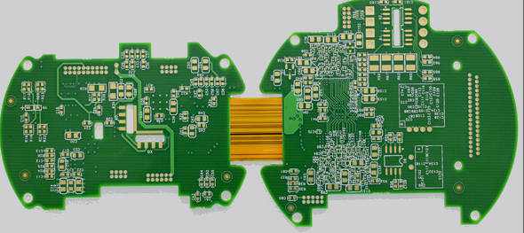
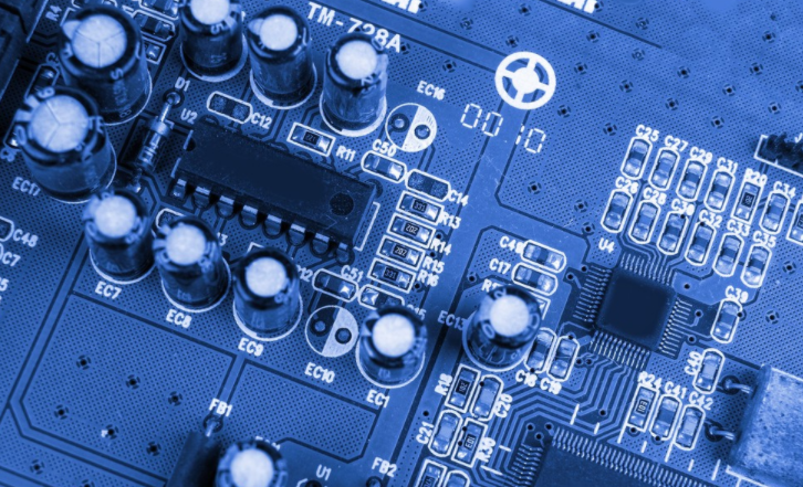
Professional PCB manufacturing and assembly
Building 6, Zone 3, Yuekang Road,Bao'an District, Shenzhen, China
+86-13410863085Mon.-Sat.08:00-20:00

Why is it difficult to tin QFN side in SMT chip processing?
QFN means square flat no pin package, which is one of SMT surface mount component packages. After SMT patch processing and welding, why does the pad around the side of QFN not receive tin or the tin climbing height cannot meet the customer's requirements? This is a long-term problem and headache for SMT personnel. Next, the SMT chip processing factory will share with you why it is difficult to tin the QFN side? How to solve it? I hope to bring you some help!
Due to the preciseness of processing technology, many SMT practitioners believe that the soldering of QFN side pad should be as full as that of QFP pin, which means the soldering is normal, while the exposed copper on QFN side is not covered by solder, which means the soldering is abnormal. In fact, this is also wrong. The tin coating of QFN is mainly determined by the welding effect at the bottom of the body. As for the amount of tin climbing on the side, it is generally the customer's requirement. IPC-A-610 standard QFN side pad tin climbing requirements are divided into three grades; Level 1: the bottom of QFN pad is obviously wetted with tin; Level 2 is 25% of the height of the side pad; Level 3 standard is 50% of the side pad height;
1、 Why is it difficult to tin the side of QFN?
Since the welding ends of the side pins of QFN are all bare copper, and the chemical reaction of copper in the air 2Cu+O2=2CuO produces copper oxide, it is known that there is a similar surface treatment method PCB called "bare copper plate", which is easy to be affected by acid and humidity and cannot be kept for a long time. After unpacking, it needs to be used up within 4 hours, otherwise the copper exposed in the air will be oxidized, thus affecting the welding quality. Similarly, if the side tin climbing of QFN must be required, the time after the cut section of QFN is exposed to copper must be controlled. Since the transportation and storage time between QFN manufacturing and SMT chip processing is much longer than 4 hours, it is unrealistic to achieve good tin coating effect. The real reason why the side of QFN is not tinned is that the side pin of QFN is cut, and there is no soldering treatment on the surface after cutting, so there is an oxide layer

2、 Solutions
1. The steel mesh opening mode of internal cutting and external pulling can be properly adopted to reduce the cross cutting size of the pad position by internal cutting and reduce the defects such as tin bonding and bridging in the welding process. At the same time, the steel mesh opening at the QFN chip pad position is extended to increase the quantity of solder paste at the QFN pin, so as to ensure that there is enough tin in the tin climbing process;
2. Select lead-free environmental protection process QFN chip packaging solder paste. Select SAC305 or SACX0307 high temperature QFN solder paste. Powder No. 4 can be used as the powder number. There is a large amount of tin during stencil printing, which is helpful for tin climbing;
3. When the tin on the side of the QFN is poor, you can add a proper amount of soldering paste around the SMT patch before processing reflow, and the soldering effect will be significantly improved;
The above is the explanation given by the editor of pcb circuit board company. If you want to know more about PCBA, you can go to our company's home page to learn about it. In addition, our company also sells various circuit boards,
High frequency circuit board and SMT chip are waiting for your presence again.


Just upload Gerber files, BOM files and design files, and the KINGFORD team will provide a complete quotation within 24h.