
Professional PCB manufacturing and assembly
Building 6, Zone 3, Yuekang Road,Bao'an District, Shenzhen, China
+86-13410863085Mon.-Sat.08:00-20:00

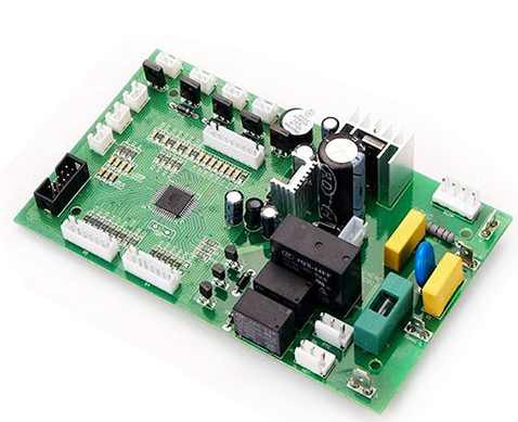
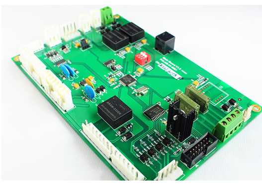
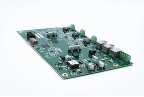
PCB DIP plug-in processing is a very important process in PCBA chip processing, and its processing quality directly affects the functional properties of , so it is necessary to pay more attention to the DIP plug-in process. DIP plug-in has a lot of preparatory work. The basic process is to process the plug-in electronic components first.
The staff will receive the materials according to BOM, check whether the material model and specification are correct, and conduct pre-processing according to PCBA template before production. The step is to use a variety of related equipment (automatic capacitance clipper, jumper bending machine, two and three audion automatic forming machine, automatic belt forming machine and other forming equipment)
for processing.

PCB DIP plug-in processing needs to pay attention to the following points:
1, before the plug-in, it is necessary to check whether the surface of the electronic components has oil stains, paint and other unclean objects.
2,In the plug-in process, it is necessary to ensure that the electronic components are flat with the PCB. After the plug-in is completed, it is necessary to ensure that the electronic components are flush, do not be uneven, and ensure that the welding pin after the plug-in can not block the welding pad.
3, if there is a direction indicator on the electronic components, it is necessary to plug in the correct direction, do not plug in at will.
4, in the plug-in, pay attention to the force of the plug-in, do not in the plug-in force is too large, resulting in damage to components or PCB board damage.
5, do not plug out the edge of the PCB board when inserting electronic components, pay special attention to the height of electronic components and the spacing between electronic components.
Our own SMT processing plant can provide SMT processing services for minimum package 0201 components. The SMT plant is equipped with 3 Fuji high-speed SMT lines, 2 DIP plug-in production lines, equipped with AOI optical detector, automatic solder paste printing machine, semi-automatic solder paste printing machine, lead-free wave soldering, lead wave soldering, upper and lower 8 temperature zone reflow welding, PCBA functional test frame, aging, board loading machine, cleaning tools, etc., at the same time, a professional research and development laboratory is set up. Five professional engineers cooperate with customers to perform general functional testing, test point testing, as well as channel, noise, waveform, drop and temperature testing.
The quality requirement for etching is the complete removal of all copper layers beneath the anti-corrosion layer. Strictly speaking, the etching quality must include the consistency of line width and the degree of side erosion.
The problem of side etching is often discussed in etching. The ratio of side etching width to etching depth is called the etching factor. In the printed circuit industry, small side etching or low etching factor is most satisfactory. The structure of the etching equipment and the different composition of the etching fluid will affect the etching factor or the degree of side erosion.
In many ways, the quality of the etching exists long before the board enters the etching machine. Because the various processes of PCB proofing have a very close internal relationship, there is no process that is not affected by other processes and does not affect other processes. Many of the problems identified as etching quality have actually existed in previous film removal processes, and even more.
In theory, PCB proofing enters the etching stage. In the pattern plating method, the ideal state should be: the total thickness of the copper and lead tin after electroplating should not exceed the thickness of the electroplated photosensitive film, so that the electroplating pattern is completely blocked by the "wall" on both sides of the film and embedded in it. However, in actual production, the plating pattern is much thicker than the photosensitive pattern; Because the coating height exceeds the photosensitive film, there is a trend of lateral accumulation. A tin or lead-tin corrosion resistant layer covering the top of the line extends to both sides to form the "edge", covering a small portion of the sensitive film below the "edge". The "edge" formed by tin or lead tin makes it impossible to completely remove the sensitive film when the film is removed, leaving a small part of the "residual glue" below the "edge", resulting in incomplete etching. After the line is etched, "copper roots" are formed on both sides, which narrow the line spacing, resulting in printed boards that cannot meet customer requirements and may even be rejected. Waste products will greatly increase the cost of PCB production.


Just upload Gerber files, BOM files and design files, and the KINGFORD team will provide a complete quotation within 24h.