
Professional PCB manufacturing and assembly
Building 6, Zone 3, Yuekang Road,Bao'an District, Shenzhen, China
+86-13410863085Mon.-Sat.08:00-20:00

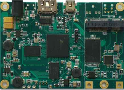
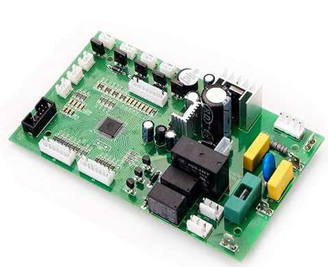
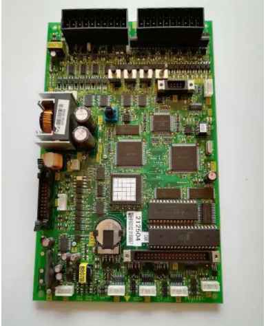
There is a very common process used in PCB proofing surface treatment, that is, the gold sinking process. So what are the benefits of the gold sinking process? The gold sinking process has very obvious characteristics.
")
First, the definition of gold
In simple terms, gold deposition is the use of chemical deposition method, through chemical REDOX reaction on the surface of the circuit board to produce a layer of metal coating.
Second, the characteristics of the gold sinking process.
The copper on the circuit board is mainly copper, copper solder joints are easy to be oxidized in the air, which will cause electrical conductivity, that is, poor tin eating or poor contact, reducing the performance of the circuit board, then you need to surface treatment of copper solder joints, gold is gilded above, gold can effectively block copper metal and air to prevent oxidation. Therefore, sinking gold is a treatment method of surface oxidation prevention, which is covered with a layer of gold on the surface of copper through a chemical reaction, also known as gold.
Third, the advantages of sinking gold surface treatment
The advantage of the gold sinking process is that the deposited color on the surface of the printed line is very stable, the brightness is very good, the coating is very flat, and the weldability is very good. The thickness of gold is generally 1-3 Uinch, so the gold thickness made by the surface treatment of gold is generally thicker, so the surface treatment of gold is widely used in circuit boards such as key boards and gold finger boards, because gold has strong electrical conductivity, good oxidation resistance and long service life.
Four, the characteristics of the gold plate
1.The sunken gold plate has bright color, good color and looks good.
2. The crystal structure formed by sinking gold is easier to weld than other surface treatments, and can have better performance and ensure quality.
3. Because the gold plate only has nickel gold on the pad, it will not affect the signal, because the signal transmission in the skin effect is in the copper layer. The metal properties of gold are relatively stable, the crystal structure is more dense, and it is not easy to oxidize.
4. Because the gold plating only has nickel gold on the pad, the welding resistance on the line is more firmly combined with the copper layer, and it is not easy to cause micro short circuit. 6. The works will not affect the spacing when making compensation. 7. The stress of the gold plate is easier to control.
Energy production from 2 layers to 14 layers, 14-22 layers can be proofing production.
Minimum line width/spacing: 3mil/3milBGA Distance :0.20MM Minimum aperture: 0.1mm inch :610mmX1200mm
Ink: Japan Tamura, Taiyo, Fudoken;
FR4: Shengyi, Kingboard, Haigang, Hongren, Guoji, Hezheng, Nanya, (Shengyi S1130/S1141/S1170),Tg130℃/ Tg170℃ T g180℃ and other high TG plates)
High frequency board: Rogers, Taconic, ARLLON; Surface process: spray tin, lead-free spray tin, sinking gold, full plate gold plating, plug gold plating, full plate thick gold, chemical sinking tin (silver), anti-oxidation (OSP) blue glue, carbon oil
kinhford Electronics is a circuit board manufacturer specializing in printed circuit board manufacturing, 20 years of focus on single, double sided, multi-layer circuit board production. Can provide FR4 hard board, FPC soft board, HDI board, metal substrate PCB proofing and mass production services.


Just upload Gerber files, BOM files and design files, and the KINGFORD team will provide a complete quotation within 24h.