
Professional PCB manufacturing and assembly
Building 6, Zone 3, Yuekang Road,Bao'an District, Shenzhen, China
+86-13410863085Mon.-Sat.08:00-20:00

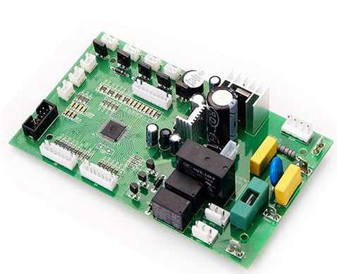
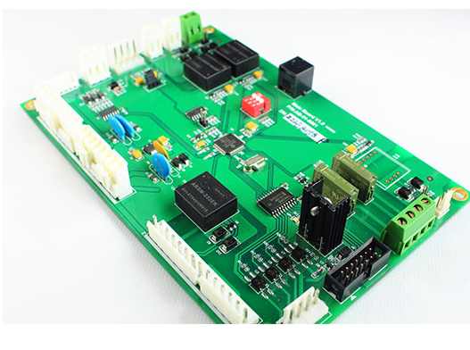
Screen printing design is an essential element of PCB design, screen printing on the PCB board usually includes: component screen printing and position number, board name, version number, anti-static identification, bar code screen printing, company LOGO and some other identifications.
")
First, screen design requirements
The ratio of word height and word width of screen printing characters is generally ≥6:1, and there are three common font sizes: among them, when the board density is relatively large, 4/25mil characters (No. 1) are commonly used; For regular density, 5/30mil characters (No. 2) are recommended; When the board is relatively loose, 6/45mil characters (No. 3) are recommended; Usually, the thickness of the surface copper base also has corresponding requirements for the screen width: the base copper < 1OZ: the limit value ≥4mil, the optimization value ≥6mil; When the base copper thickness is 1OZ, 5/30mil characters are preferred; For base copper 2OZ, 6/45mil characters are preferred.
Second, add PCB screen printing requirements
1, the position of the placement: In general, resistance, capacitance, pipe and other devices screen printing, when placed, do not use four directions, which will lead to debugging, maintenance, welding, see screen printing to see very tired (the board to turn several directions). 2. Try not to hit the screen print through the hole.
3, screen printing do not press on the high-speed signal line (such as, clock line, etc.) : for the top or bottom of the high-speed signal line, because this type of signal line can be seen as a microstrip line.
4. The reading direction of screen printing should be consistent with the direction of use. The reading direction of screen printing should be consistent with the direction of use of the chip, mainly when welding, reducing the probability of welding.
5, screen printing to mark the pin number clearly.
6. Screen printing for special packages: For special packages such as BGA and QFN, the size of screen printing should be exactly the same as the size of the chip. 7. Screen printing of the mounting hole: the screen printing of the screw is increased near the mounting hole, and the length and total number of screws are indicated, which is convenient for installation. 8, the ambiguity of screen printing: the most commonly used RS232, many people will mark RX and TX, but the PC side also has RX and TX ah, when to use a cross line, when to use no cross? This leads to ambiguity in the screen printing, which makes people stupidly indistinguishable.
Third, silk screen design precautions
1. The silk screen line width on the board is greater than or equal to 4mil, and the silk screen line width of components is avoided.
2, screen printing and pad spacing: screen printing do not cover the welding points on the board, such as patch device pad, plug-in through the hole, screen printing is an insulating material, once on the pad, will lead to poor welding; Do not cover the test points on the board, mark points, etc.; It is usually required to maintain a 6mil spacing.
3, the distance between the screen printing: keep 6mil, it is acceptable to have a coincidence between the screen printing, once the coincidence can not be identified, you need to open.
4, silk screen direction: silk screen string arrangement should follow: face the string from left to right or from bottom to top principle.
5, the device position number: the device position number should correspond to the device one by one, can not be reversed, transform the order; When the device density is relatively high, the bit number can be placed in other places with space on the board by using the method of lead marking or symbol marking.
6, the component polarity mark and "1" foot mark should be placed correctly and clearly.
7, When drawing out the mark or symbol mark, the added screen printing and characters should be placed on the screen printing layer of Board Geometry. The added screen print of the Board name version number is also placed on the screen layer of the Board Geometry.
8, the device position number can not be placed in the device body or outside the frame.
9, when the board density is relatively high, there is no space to place the number, you can discuss with the customer not to place the number, but the need for assembly drawings to facilitate the installation and inspection of the device.
10, when the customer requires the top bottom to write copper words, line copper word line width: HOZ base copper: character width of more than 8mil, height of more than 45mil; 1OZ base copper: more than 10mil character width; Height above 50mil. At the same time, it is necessary to do a good job of welding resistance window, so that the copper words on the board produced are brighter.
kingford Electronics is a professional PCB design company engaged in electronic product circuit board design (layout layout design), mainly undertake multi-layer, high-density PCB design and circuit board design proofing business. With an average of more than 10 years of work experience in PCB design team, can skillfully use the market mainstream PCB design software, professional and efficient communication to ensure PCB design progress, to help you seize the market opportunity one step earlier!


Just upload Gerber files, BOM files and design files, and the KINGFORD team will provide a complete quotation within 24h.