
Professional PCB manufacturing and assembly
Building 6, Zone 3, Yuekang Road,Bao'an District, Shenzhen, China
+86-13410863085Mon.-Sat.08:00-20:00

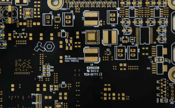
The principles of the layout of components in the SMT process:
1. For double-sided mounted components, the larger devices on both sides should be staggered in the installation position, otherwise the welding effect will be affected by the increase of local heat capacity during the welding process.
2, when the circuit board is placed on the conveyor belt of the reflow welding furnace, the long axis of the components should be perpendicular to the transmission direction of the equipment, which can prevent the phenomenon of components drifting on the board or "erecting tablets" during the welding process.
3. Devices with pins on four sides such as PLCC/QFP cannot be placed on the wave crest welding surface.
4, the components on the PCB should be evenly distributed, especially the high-power devices should be dispersed to avoid local overheating stress on the PCB when the circuit is working, affecting the reliability of the solder joint.
5, the large and small SMT components on the wave crest welding surface can not be arranged in a straight line, and the positions should be staggered, which can prevent virtual welding and welding leakage caused by the "shadow" effect of the solder crest during welding.
6, the SMT large device installed on the crest welding surface, its long axis should be parallel to the direction of the solder crest flow, which can reduce the solder bridge between the electrodes.

The problem of holes in solder joints in SMT processing
Compared with tin-lead solder, lead-free solder joints are more likely to form voids, and the percentage of voids in SAC alloys is higher than that of other lead-free alloys. The phenomenon of holes seen in the X-ray film may be one of the factors that mark the solder joint as unqualified, which is recognized in the electronics manufacturing industry. There has always been A certain amount of controversy in the electronic assembly industry, with the transition to lead-free, more and more controversy, mainly because lead-free solder joints are more likely to form holes than tin lead solder in the IPC SPVC test project using two types of lead-free circuit boards for testing: lead-free test board A* and lead-free test board B**. The solder paste used for both test plates is not specially selected, but the same flux is used.
In the lead-free test board A*, holes of more than 25% were seen on all boards assembled with three SAC alloy solder pastes, especially CSP84 lead-free components with a spacing of 0.5mm. There is a significant void in the board assembled with tin-lead alloy, but the void area is less than 25% on the CSP84 component assembled with tin-lead alloy with a spacing of 0.5mm. The thermal shock test protocol is very similar to that specified by JEDEC, which is first maintained at a low temperature (-55 ° C) for five minutes, then at a high temperature (125 ° C) for ten minutes, and then back to the low temperature. The total cycle time is about 20 minutes. This cycle is repeated continuously. The metallographic analysis was carried out after 500 temperature cycles for each of the two sets of test pieces. The test boards included boards from two companies, each with four sets of forty boards, each using three SAC solder alloys and a low-melting (tin-lead) solder for comparison. Each group performed a destructive metallographic analysis on a plate that did not participate in the temperature cycle study.
To determine the impact of voids on the reliability of solder joints, IPC SPVC uses a test protocol that includes routine temperature cycling and thermal shock that is accepted throughout the industry. Environmental tests were carried out on both sets of test boards, during which their functions were monitored. The test boards included boards from two companies, each with four sets of forty boards, each using three SAC solder alloys and a low-melting (tin-lead) solder for comparison. Each group performed a destructive metallographic analysis on a plate that did not participate in the temperature cycle study. On the lead-free test board B**, holes of more than 25% were seen on all boards assembled with SAC alloy. On the board, the holes of PBGA196, C-CSP224 and the chell-scale package CSP8 are almost more than 25%.
The temperature cycle scheme used mirrors the IPC test method. This temperature cycle scheme is first maintained at a low temperature (0 ° C) for ten minutes, then the temperature slowly rises to 100 ° C, and then at this high temperature for ten minutes, and then gradually returns to the low temperature state. The entire temperature cycle usually takes about 60 minutes. The cycle time is related to the time of furnace temperature rise and the temperature stabilization process of the test plate.


Just upload Gerber files, BOM files and design files, and the KINGFORD team will provide a complete quotation within 24h.