
Professional PCB manufacturing and assembly
Building 6, Zone 3, Yuekang Road,Bao'an District, Shenzhen, China
+86-13410863085Mon.-Sat.08:00-20:00

"Highly integrated miniaturization and modularity are the technical requirements for the development of downstream electronic products, and also the general trend of printed circuit board (PCB) to fully support the development of the electronics industry", when talking about the innovative technology trend of high-end PCB development, Mr. Zhengqiang Pan, CEO and General manager of China region of OTus Group Mobile Devices and Packaging Board Division, said. "With the application of new technologies such as embedded component packaging and system level packaging (SiP) in high-end iot, medical electronics, wearable devices, industrial automation solutions, vehicle networking and driverless, Orteus will continue to regard technology as the core driving force and provide cutting-edge technology industrialization solutions with rich technical capabilities."
Recently, Ortex released the financial results for the first half of 2015/2016, maintaining the encouraging trend of continued rapid development, sales rose 28.2% to 387.1 million euros. This data once again exceeded the industry's average level of single-digit growth, making the industry sit up and take notice. Today, with the rapid growth of all kinds of electronic products slowing down, how to continue to ensure the secret of high sales growth has become the focus of EDN China's hope to discuss with Otus.

Regarding the high growth, Mr. Ankailer, Chief financial Officer of Otes Group, said: "This is mainly due to the increase in demand for high-end PCBS from our customers in the first six months, which is also in line with Otes' high-end focus. The first half of the year did not show the usual seasonal fluctuations. At the same time, the favorable exchange rate contributes to the growth of sales, while the impact of positive and negative exchange rate deviations on earnings basically cancels each other out. We saw strong growth in our mobile devices and automotive businesses as well as excellent capacity utilisation at our plants, including in Shanghai."
As for how to continue to maintain the high growth plan in the future, Mr. Pan Zhengqiang, CEO and Managing director of China of OTus Group's Mobile Equipment and loading Board Division, said, "OTus has invested in two advanced PCB and carrier technologies in Chongqing plant, which will ensure Otus's industry leadership and long-term profit growth." The construction of the Chongqing plant is well underway, and is expected to be certified by the end of this year, which will gradually start mass production scheduled to start early next year. The two plants will respectively manufacture semiconductor sealing plates (Chongqing Plant 1) and systems-level packaging PCBs (Chongqing Plant 2). To further meet the growing customer demand for advanced applications and high-quality products."
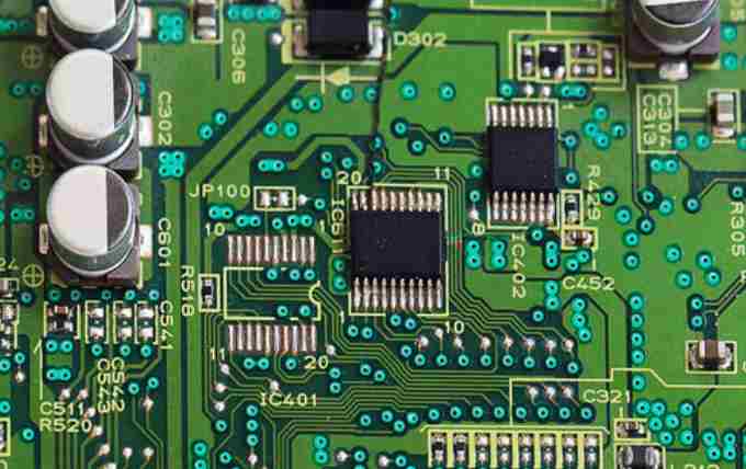
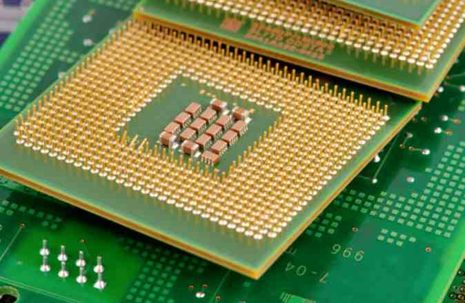
Semiconductor cap board and System Level Package PCB (SLP)
Stratification from a technical point of view, about 70% of the current market structure of PCB is single-sided, double-sided, multi-layer, soft board or soft and hard composite board including auxiliary technology, while high-end HDI PCB or semiconductor seal loading board accounted for only 30%, and for Otes, the technical layout is just the opposite. Pan Zhengqiang introduced: "The company's positioning is mainly high-tech, 70% of the turnover is from HDI, as well as higher-end arbitrary layer PCB, embedded technology (that is, the semiconductor embedded in our PCB technology)." These account for more than 70% of the company. The remaining 30 percent is less than traditional technology that we assist."
As early as 2011, Otus decided to invest in a second factory in Chongqing, and plans to invest a total of 624 million US dollars by mid-2017 for the Chongqing plant, which mainly provides semiconductor seal loading plates for microprocessors. Scheduled for (production in early 2016) and System level sealing and loading plates (SLP) for wearable devices and high-end iot applications (Plant 2, scheduled for production in late 2016).
For the progress of the Chongqing plant, Pan Zhengqiang introduced that the current can be said to be the last quarter of the long march: "As of September 30, 2015, a plant has invested 182.4 million euros, the current parameter setting and qualification certification of the first production line is in progress, and it is expected to be certified by the end of 2015, and the product line is supporting customers in the leading position in the semiconductor industry. The main product portfolio is FCBGA sealing plates for computer applications (notebooks, personal computers, etc.). Production is expected to start in early 2016 and the cost of production will affect the 2015/16 Q4."
The second plant, mainly for the production of SLP, is also under construction, and the plant has been capped on October 29, 2015. "System-level packaging of printed circuit boards is an important step for Ortex to invest in the next generation of innovative PCB technology. With an investment of €13.9 million, the first SLP has already been produced in Shanghai and production of the SLP at Chongqing 2 is expected to begin in the second half of 2016."
For SLP technology, Pan Zhengqiang also added: "SLP, or the so-called SIP, is currently mainly developed by OtUS itself. This product is between our highest end HDI and the sealing plate, there is a technical gap, filling this gap is our so-called SLP technology. If the technical requirements such as line width and line distance are not the requirements of high-end sealing plates, but it is also higher than the so-called arbitrary layer HDI, there is a middle point.
Embedding technology can be used in HDI, sealing plates, or SLP. The application of this technology mainly depends on whether the product design needs to be so small. If the product does not have enough space, it must be made smaller, which can be carried out with technologies such as SLP embedding. In this regard, the Shanghai factory has already produced the first SLP for a wearable product application."


Just upload Gerber files, BOM files and design files, and the KINGFORD team will provide a complete quotation within 24h.