
Professional PCB manufacturing and assembly
Building 6, Zone 3, Yuekang Road,Bao'an District, Shenzhen, China
+86-13410863085Mon.-Sat.08:00-20:00

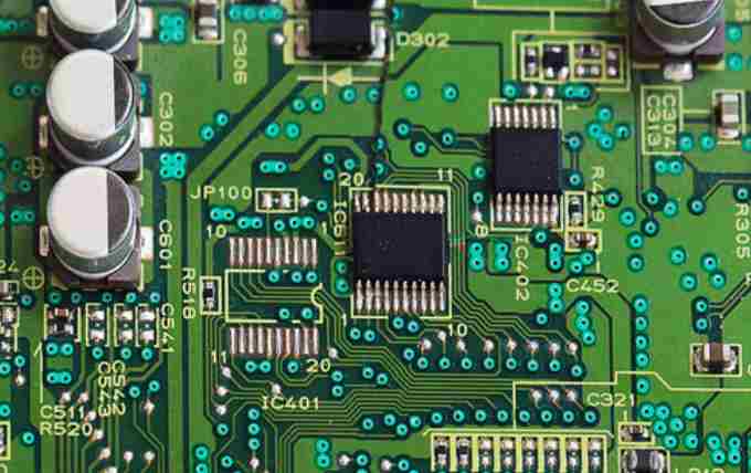
SMT chip processing is a Surface assembly Technology (surface Mounted technology) (Surface Mounted Technology), is currently the most popular technology and process in the electronic assembly industry. SMT patch processing refers to a series of processes that are processed on the basis of PCB. PCB (Printed Circuit Board) means printed circuit board.
SMT patch processing common printing defects and solutions
First, pull the tip
The pull point is the solder paste on the pad after printing is small, which may be caused by the scraper gap or the solder paste viscosity is too large. Prevention or solution: adjust the gap of the scraper appropriately or choose the appropriate viscosity of the solder paste.
Second, the thickness is inconsistent
After printing, the thickness of the solder paste on the pad is inconsistent, which causes:
1. The template is not parallel to the printed board;
2, the solder paste stirring is not uniform, so that the particle size is inconsistent.
Prevention or solution: adjust the relative position of the template and the printed board; Stir the solder paste thoroughly before printing.

3. Collapse
After printing, the solder paste collapses to both sides of the pad. Cause:
1. The pressure of the scraper is too large;
2, the printed board positioning is not strong;
3, the solder paste viscosity or metal content is too low.
Prevention or solution: Adjust the pressure; Refixing the printed board; Select a solder paste with the right viscosity.
4. There are burrs on the edges and surfaces
The reason may be that the viscosity of the solder paste is low and the wall of the template is rough.
Prevention or solution: choose a solder paste with slightly higher viscosity; Check the etching quality of template openings before printing.
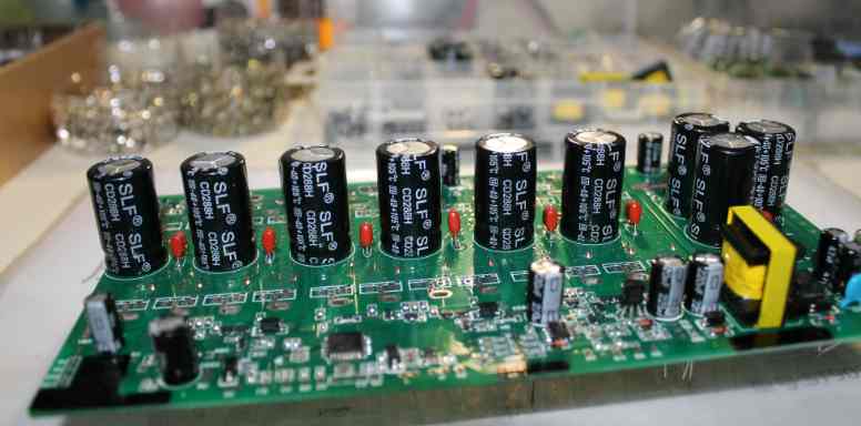
SMT patch processing The component is pasted to the PCB printed with glue or solder paste through the device, and then through the welding furnace, which is the patch processing.
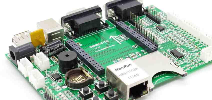
PCB board size considerations
When the selected processing process involves a milling cutter cutter, the PCB board size is 70mm×70mm -- 310mm×240mm.
When the selected processing process involves the circular knife cutting machine, the PCB panel size is 50mm×50mm (taking into account the processing capacity of other equipment) - 450mm×290mm. Plate thickness: 0... 8mm -- 3.2mm.
When the selected processing process does not involve the cutting machine (such as network products), the PCB board size: 50mm×50mm -- 457mm×407mm. (wave soldering), plate thickness: 0.5mm -- 3.0mm. For details, see appendix "Processing Equipment Parameter Table". Special attention should be paid to the processing capacity of the equipment when making the process fixture.
Process edge
At least one pair of sides on the PCB board should leave enough space for the location of the conveyor belt, that is, the process edge. PCB board processing, usually use the long opposite side as the process side, left for the conveyor belt of the equipment, in the conveyor belt can not have components and lead interference, otherwise it will affect the normal transmission of the PCB board.
The width of the process edge is not less than 5mm. If the layout of the PCB board cannot be met, the method of adding auxiliary edges or panels can be used, see "panels".
PCB test impedance process edge is greater than 7MM.
PCB board made arc Angle
Right-angle PCB board is easy to produce a card during transmission, so when designing PCB board, it is necessary to do arc Angle processing on the board frame, and determine the radius of arc Angle (5mm?) according to the size of the PCB board. . The assembled board and the PCB board with auxiliary side make arc Angle on the auxiliary side.
Safe distance between components
Considering that there is a certain error when the machine is mounted, and considering the convenience of maintenance and visual appearance inspection, the adjacent two component bodies can not be too close, and a certain safe distance should be left.
QFP, PLCC------
The common feature of these two devices is the four-sided lead package, the difference is that the lead shape is different. QFP is a gull-wing lead and PLCC is a J-shaped lead. Because it is a four-sided lead package, the wave soldering process cannot be used.
QFP and PLCC devices are usually distributed on the component surface of the PCB board, and if they are to be distributed on the welding surface for the secondary reflow welding process, their weight must meet the requirements of: the weight of the contact surface of the welding Angle should be less than or equal to 30 grams per square inch.
BGA equiplanar array device -----
BGA and other planar array devices are used more and more, and 1.27mm, 1.0mm and 0.8mm ball pitch devices are commonly used. The device layout of the BGA iso-plane array is mainly concerned with its maintainability. Due to the space limitation required by the hot air hood of the BGA repair table, no other components can be located within 3mm around the BGA. In normal cases, the BGA equiplanar array device is not allowed to be arranged on the welded surface. If the layout space is limited, the weight of the BGA equiplanar array device must meet the preceding requirements.
BGA equiplanar array devices cannot adopt wave soldering process.
SOIC device
There are many forms of small-shape package devices, such as SO, SOP, SSOP, TSOP, etc., and their common feature is the edge lead package. These devices are suitable for reflow welding processes and have the same layout design requirements as QFP devices. For SOIC devices with Standoff distance ≥1.27mm (50mil) and standoff height ≤0.15mm, wave soldering can be adopted. However, it is necessary to pay attention to the relative direction between the SOIC device and the wave peak.
Standoff larger than 0.2mm cannot cross the standoff peak
SOT, DPAK devices
SOT devices are suitable for reflow soldering and wave soldering processes, and can be placed on the component surface and the weld surface during layout. When using the Standoff welding process, the standoff height should be less than 0.15mm.


Just upload Gerber files, BOM files and design files, and the KINGFORD team will provide a complete quotation within 24h.