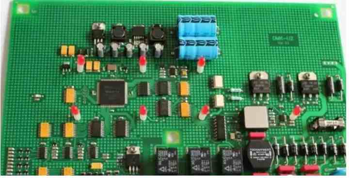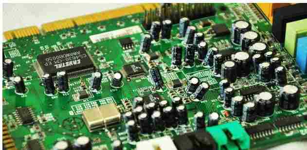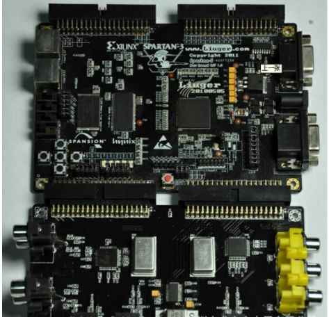
Soft and hard PCB design points, that is, flexible circuit board and hard circuit board, after pressing and other procSoft and hard combined boardesses, according to the relevant process requirements combined together to form a circuit board with FPC characteristics and PCB characteristics. There are many differences in PCB design between soft board and hard board.
1, flexible area line design requirements:
1.1 line to avoid sudden expansion or contraction, thick and thin line between the tear shape;
1.2 In the case of meeting the electrical requirements, the welding pad should be the maximum value, and the connection between the welding pad and the conductor should use a smooth transition line, avoid using a right Angle, and the independent welding pad should be added to the toe, so as to strengthen the support.
2, dimensional stability: add copper design as much as possible, and design as many solid copper foils as possible in the scrap area.
3.1 Increase manual alignment holes to improve alignment accuracy
3.2 Window design Considering the range of glue flow, usually the window opening is larger than the original design, the specific size provided by ME design standards
3.3 Small and dense window opening can use special mold design: rotary punching, jump punching, etc. 4. Design of rigid torsion transition zo

4. Design of rigid torsion transition zone
4.1 Smooth transition of the line, the direction of the line should be perpendicular to the bending direction
4.2 The wire should be evenly distributed throughout the bending zone
4.3 The width of the wire should be maximized throughout the bending zone.
4.4 PTH design should not be adopted in the transition area.
4.5 Design of rigid flexible transition zone Coverlay and NoflqwPP
5. Design of flexible zone with air-gap requirements
5.1 There should be no through hole in the part to be bent;
5.2 Add protection copper wire to the most sides of the line. If there is insufficient space, choose to add protection copper wire to the inner R Angle of the bent part.
5.3 The connection part of the line should be designed as an arc.
5.4 The larger the bent area is, the better, without interfering with the assembly.
6. Tool holes of other soft boards cannot be shared, such as punch holes, ET holes, and SMT positioning holes.
Soft and hard board PCB design precautions
1, the separation distance of the large-area mesh of the soft and hard bonding board is too small, in the process of printed circuit board production and manufacturing, the diagram transformation process will be very easy to produce a lot of broken film attached to the board, resulting in broken lines.
2,The setting of the aperture of the single-sided pad of the soft and hard bonding plate is not perfect, and there will be problems in the process of drilling.
3, the electric formation of the soft and hard combination plate is the problem of welding pad and connection.
4, in the design process of the soft and hard bonding plate, the overlap of the pad, because after the hole overlap, the drilling process will be due to multiple drilling in a place to break the drill bit, resulting in hole damage.
kinhford Electronics is a circuit board manufacturer specializing in printed circuit board manufacturing, 20 years of focus on single, double sided, multi-layer circuit board production. Can provide FR4 hard board, FPC soft board, soft and hard board, HDI board, metal substrate and other PCB proofing and mass production services.


