
Professional PCB manufacturing and assembly
Building 6, Zone 3, Yuekang Road,Bao'an District, Shenzhen, China
+86-13410863085Mon.-Sat.08:00-20:00

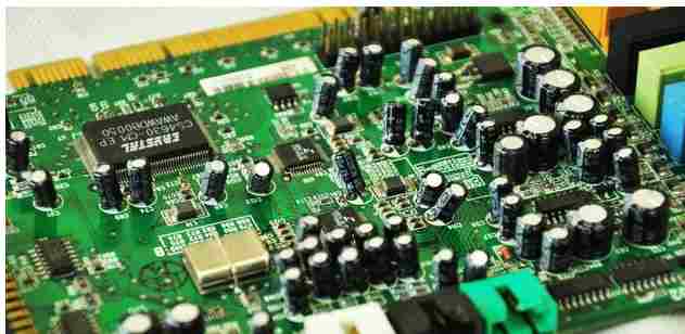
In the PCB design and wiring rules, there is a principle of "key signal line priority", that is, key signals such as power supply, analog signals, high-speed signals, clock signals, differential signals and synchronous signals are prioritized. First, analog signal wiring requirements
The main feature of analog signal is poor anti-interference, and the protection of analog signal is mainly considered when wiring.
The processing of analog signals is mainly reflected in the following points:
1,In order to increase its anti-interference ability, the line should be as short as possible.
2,Some analog signals can abandon the impedance control requirements, and the wiring can be appropriately bolded.3. Limit the wiring area, try to complete the wiring in the analog area, away from the digital signal.
Second, high-speed signal wiring requirements
Multi-layer wiring
High speed signal wiring circuit often has high integration and high wiring density, the use of multilayer board is not only necessary for wiring, but also an effective means to reduce interference. Reasonable selection of layers can greatly reduce the size of the printing board, can make full use of the middle layer to set the shield, can better realize the nearby grounding, can effectively reduce the parasitic inductance, can effectively shorten the transmission length of the signal, can greatly reduce the cross interference between the signals.
The less the lead bends, the better
The less lead bending between pins of high-speed circuit devices, the better. High-speed signal wiring circuit wiring lead is best to use a straight line, need to turn, can be used 45° line or arc turn, this requirement in the low-frequency circuit is only used to improve the strength of steel foil fixation, and in the high-speed circuit, to meet this requirement can reduce the high-speed signal external emission and mutual coupling, reduce signal radiation and reflection.
The shorter the lead, the better
The shorter the lead between the pins of the high-speed signal routing circuit device, the better. The longer the lead, the larger the value of the distributed inductance and distributed capacitance, which has a lot of influence on the passing of the high-frequency signal of the system, and also changes the characteristic impedance of the circuit, resulting in reflection and oscillation of the system.
The less alternations between lead layers, the better
The less interlayer alternations between pins of high-speed circuit devices, the better. The so-called "the less interlayer alternations of the leads, the better" means that the fewer holes used in the connection process of the components, the better. It has been measured that a pass hole can bring about 0.5pf of distributed capacitance, resulting in a significant increase in the delay of the circuit, and reducing the number of pass holes can significantly improve the speed.
Pay attention to parallel cross interference
High-speed signal wiring should pay attention to the "cross interference" introduced by the signal line in the short distance parallel line, if the parallel distribution cannot be avoided, a large area of "ground" can be arranged on the opposite side of the parallel signal line to greatly reduce the interference.
Avoid branches and stumps
High-speed signal wiring should try to avoid branching or forming a Stub. Stumps have a great impact on impedance and can cause signal reflection and overshoot, so we should usually avoid stumps and branches in the design. Using Daisy chain wiring, the impact on the signal will be reduced.
The signal line should go as far as possible in the inner layer.
The high-frequency signal line walking on the surface is easy to produce large electromagnetic radiation, and it is also easy to be interfered by external electromagnetic radiation or factors. The high-frequency signal line is routed between the power supply and the ground wire, and the radiation generated will be reduced a lot through the absorption of electromagnetic waves by the power supply and the bottom.
Three, clock signal wiring requirements
In digital circuit design, the clock signal is a signal that oscillates between high and low states and determines the performance of the circuit. Clock circuit plays an important role in digital circuit midpoint, and is also the main source of electromagnetic radiation. The processing method of the clock also needs special attention when PCB wiring. By clarifying the clock tree at the beginning and clarifying the relationships between the various clocks, you can handle the wiring better. And the clock signal is often the difficulty of EMC design, and the project that needs to pass the EMC test index should pay particular attention.
In addition to the conventional impedance control and isometric requirements of the clock line, the following issues need to be noted:
1. Choose the optimal routing layer for clock signals as far as possible.
2. The clock signal should not cross the division as far as possible, let alone route along the division area.
3. Pay attention to the distance between the clock signal and other signals, at least 3W.
4. There are EMC requirements of the design, long line as far as possible to choose the inner wiring.
5. Match the end connection of the clock signal.
6. Do not use the Daisy chain structure to transmit the clock signal, but should use the star structure, that is, all the clock load is directly connected to the clock power driver.
7. All wires connected to the input/output end of the crystal oscillator should be as short as possible to reduce noise interference and the influence of distributed capacitance on the crystal oscillator.
8. The crystal capacitor ground wire should be connected to the device with as wide and short a wire as possible; The digital ground pin closest to the crystal oscillator should minimize holes.
9. In digital circuits, the usual clock signals are signals with fast edge changes and large external crosstalk. Therefore, in the design, the clock line should be surrounded by the ground line and more ground lines to reduce the distributed capacitance, thereby reducing crosstalk; For the high frequency signal clock, try to use the low voltage off time clock signal and pack the ground, and pay attention to the integrity of the pack hole.
Four, differential signal wiring requirements
Differential signals, also known as differential signals, use two identical, opposite polarity signals to transmit one data, relying on the level difference between the two signals for judgment. In order to ensure that the two signals are completely consistent, they should be kept parallel when wiring, and the line width and line spacing should remain unchanged.
Five, PCB design key signals how to route
")
On the board, the differential wiring must be two wires of equal length, equal width, close together, and at the same level.
1. Equal length: Equal length means that the length of two lines should be as long as possible, in order to ensure that the two differential signals maintain opposite polarity at all times. Reduce common mode components.
2. Equal width isometric: Equal width means that the line width of the two signals needs to be consistent, and equal distance means that the spacing between the two lines should remain unchanged and remain parallel.
Reminder: Try to provide a special wiring layer for key signals such as clock signals, high-frequency signals, and sensitive signals, and ensure its minimum loop area. The signal quality is guaranteed by means of shielding and increasing safety distance.
kinhford Electronics is a professional PCB design company engaged in electronic product circuit board design (layout layout design), mainly undertake multi-layer, high-density PCB design and circuit board design proofing business. With an average of more than 10 years of work experience in PCB design team, can skillfully use the market mainstream PCB design software, professional and efficient communication to ensure PCB design progress, to help you seize the market opportunity one step earlier!
Soft and hard combined board
Jun 17,2023


Just upload Gerber files, BOM files and design files, and the KINGFORD team will provide a complete quotation within 24h.